Soft Nanoscience Letters
Vol.05 No.04(2015), Article ID:60382,9 pages
10.4236/snl.2015.54007
Optical and Electrical Properties of Nanocrystalline SnO2 Thin Films Synthesized by Chemical Bath Deposition Method
Suresh Sagadevan1*, Jiban Podder2
1Department of Physics, AMET University, Chennai, India
2Department of Chemical and Biological Engineering, University of Saskatchewan, Saskatoon, Canada
Email: *drsureshnano@gmail.com
Copyright © 2015 by authors and Scientific Research Publishing Inc.
This work is licensed under the Creative Commons Attribution International License (CC BY).
http://creativecommons.org/licenses/by/4.0/


Received 5 September 2015; accepted 17 October 2015; published 20 October 2015
ABSTRACT
The chemical bath deposition (CBD) technique was used for the synthesis of the tin oxide (SnO2) thin films. X-ray diffraction (XRD) was employed to find the crystallite size by using Debye Scherrer’s formula. The surface morphology of SnO2 films was analyzed by the scanning electron microscopic (SEM) studies. The FT-IR spectrum exhibits the strong presence of SnO2. The optical properties of the SnO2 thin films were determined using UV-Visible spectrum. The dielectric studies were carried out at different frequencies and at different temperatures for the prepared SnO2 thin films. Further, electronic properties, such as valence electron plasma energy, average energy gap or Penn gap, Fermi energy and electronic polarizability of the SnO2 thin films, were determined. The ac conductivity of the SnO2 thin films increases with increase in temperature and frequency. The activation energy was determined by using dc electrical conductivity measurement. The Hall properties were also calculated.
Keywords:
SnO2, CBD, XRD, SEM, FTIR, and Dielectric Studies

1. Introduction
Currently, the development goes hand in hand with the explosion of scientific and technological breakthrough in micro electronics, optoelectronics and nanotechnology. Tin dioxide is a n-type wide-band gap semiconductor (Eg = 3.6 eV) [1] . The SnO2 films have several potential applications such as in transparent electrodes, film resistors, electric conversion films, heat-reflective mirror, far-infrared detectors and high-efficiency solar cells [2] . The SnO2 thin films are synthesized by a variety of methods such as RF magnetron sputtering, metal organic chemical vapor deposition, vacuum evaporation, pulsed laser deposition, pulsed electron beam deposition, spray pyrolysis, sol-gel, chemical vapor deposition, and successive ionic layer adsorption and reaction, CBD [3] - [13] . CBD is an excellent method to deposit nanocrystalline thin films. The CBD technique is based on the slow controlled precipitation of the desired compound from its ions from reaction bath solution on the substrate surface. In the present investigation, nanocrystalline SnO2 thin films were prepared by using a simple CBD method. The prepared films were characterized for their structural surface morphology, optical properties, and electrical studies using XRD, FTIR, SEM, UV-visible spectroscopy, and Hall measurement.
2. Materials and Methods
2.1. Preparation of SnO2 Thin Films
SnO2 thin films were prepared on commercial microscopic glass slide by using the CBD technique. The substrates were washed using soap solution and subsequently kept in hot chromic acid and then ultrasonically cleaned with deionized water for 10 min and wiped with acetone and stored in a hot oven. The deposition bath consisted of an aqueous solution of (0.1 M) tinchloride dihydrate, (0.5 M) hydrogen peroxide, (0.5 M) triethanolamine, (0.1 M) ethylenediaminetetraacetic acid solution and deionized water. 20 mL of tin chloride dihydrate solution was mixed with 3 mL triethanolamine in a 100 mL beaker. A homogenous solution was obtained after stirring for several minutes. Then, 5 mL ethylenediaminetetraacetic acid and 5 mL hydrogen peroxide were added under stirring. Finally, deionized water was added to make the volume up to 50 mL. The deposition was carried out at temperature 110˚C. The pH of the solution was about 7 using ammonia and very slow stirring was given to the solution during the deposition. A glass substrate was placed vertically inside the vessel with the help of a suitably designed substrate holder. After a time period of 30 min, the glass slide was removed from the bath and cleaned with deionized water and dried in the hot oven. Many trials were made by optimizing the deposition parameters to obtain a good quality SnO2 thin film. The resultant films were found homogeneous and well adhered to the substrate with mirror like surface. The deposited good quality SnO2 thin films were subjected to characterization studies.
2.2. Characterization Techniques
The XRD pattern of the SnO2 thin films was recorded by using a powder X-ray diffractometer (Schimadzu model: XRD 6000 using CuKα (λ = 0.154 nm) radiation, with a diffraction angle between 20˚ and 70˚. The crystallite size was determined from the broadenings of corresponding X-ray spectral peaks by using Debye Scherrer’s formula. Scanning Electron Microscopy (SEM) studies were carried out on JEOL, JSM-67001. The FTIR spectrum of the SnO2 thin film was taken using an FTIR model Bruker IFS 66W Spectrometer. The optical absorption spectrum of the SnO2 thin films was taken by using the VARIAN CARY MODEL 5000 spectrophotometer in the wavelength range of 300 - 900 nm. The dielectric properties of the SnO2 thin films were analyzed using a HIOKI 3532-50 LCR HITESTER over the frequency range 50 Hz - 5 MHz. The Hall measurements were carried out using van der Pauw configuration (ECOPIA HMS-3000) at room temperature.
3. Results and Discussion
3.1. Structural Characterization
The XRD pattern of the SnO2 thin films was recorded by using a powder X-ray diffractometer, with a diffraction angle between 20˚ and 70˚. The XRD pattern of the SnO2 thin films is shown in Figure 1. The strong and sharp diffraction peaks indicate the formation of well crystallized SnO2 thin films. It can be seen that the major peak (110) is dominating the other peaks. The XRD results reveal that the deposited SnO2 thin films are polycrystalline in nature with having (110) plane as the preferred growth orientation. The average crystalline size (D) was calculated using the Debye-Scherrer formula,
 (1)
(1)

Figure 1. XRD spectrum of SnO2 thin films.
where λ is the X-ray wavelength, θ is the Bragg diffraction angle, and β is the FWHM of the XRD peak appearing at the diffraction angle θ. The average crystalline size was calculated from X-ray line broadening peak and Debye-Scherrer equation to be about 18 nm.
3.2. Surface Morphology
Surface morphology is an important property to understand growth surface of the deposited layers and surface roughness of the thin film. Figure 2 shows the SEM image of the SnO2 thin films. The SnO2 thin films showed a smoother surface morphology. The SnO2 micrograph shows a compact structure composed of a single type of small, densely packed microcrystals. The grains are well defined, spherical and of almost similar size. The mean crystallite size was found to be about ~16 nm.
3.3. FT-IR Studies
The FT-IR absorption spectrum of SnO2 thin films is shown in Figure 3. The FT-IR spectrum of SnO2 shows strong peak at 674 cm−1 corresponding to the characteristic antisymmetric stretching vibrations for Sn-O-Sn. The peak at 610 cm−1 corresponds to the characteristic stretching vibrations of Sn-O. Besides, the broad peaks at 3400 and 1020 cm−1 observed which are attributed to the O-H stretching vibrations. The absorption peak at around 1633 cm−1 is due to the bending vibration of hydroxyl groups of molecular water.
3.4. UV-Visible Spectroscopy
The optical absorption spectrum of the SnO2 thin films was taken in the wavelength range of 300 - 900 nm. Figure 4(a) shows the variation of the optical absorbance with the wavelength of the SnO2 thin film. From this figure, the edge is found to be shifted towards longer wavelength region (red shift). The fundamental absorption corresponding to the optical transition of the electrons from the valence band to the conduction band can be used to determine the nature and value of the optical band gap Eg of the films.
The optical absorption coefficient (α) was calculated from transmittance using the following relation
 (2)
(2)
where T is the transmittance and d is the thickness of the films. The films under study have an absorption coefficient (α) obeying the following relation for high photon energies (hν)
 (3)
(3)
where Eg is the optical band gap of the films and A is a constant. A plot of variation of (αhν)2 versus hν is shown

Figure 2. SEM micrograph of SnO2 thin film.

Figure 3. FTIR spectrum of SnO2 thin film.

Figure 4. (a) Optical absorption spectrum of SnO2 thin film (b) Plot of (αhν)2 versus hν The optical absorption coefficient (α) was calculated from trans- mittance using the following relation.
in Figure 4(b). Eg is evaluated using the extrapolation of the linear part. The intercept on energy axis gives the value of band gap energy found to be 3.5 eV. The wide band gap and minimum absorbance of deposited SnO2 thin film in the UV-Visible range indicates the potential application of prepared thin films as window layer in solar cell device [14] .
Determination of Optical Constants
Two of the most important optical properties, namely the refractive index (n) and the extinction coefficient (K) are generally called optical constants. The amount of light that transmits through thin film material depends on the amount of the reflection and the absorption that take place along the light path. The optical constants such as the refractive index (n), the real dielectric constant (er) and the imaginary parts of dielectric constant (ei) were calculated.The extinction coefficient (K) could be obtained from the following equation
 (4)
(4)
The extinction coefficient (K) was found to be 0.0032 at λ = 900 nm. The transmittance (T) is given by
 (5)
(5)
Reflectance (R) in terms of absorption coefficient could be obtained from the above equation.
Hence,
 (6)
(6)
Refractive index (n) could be determined from reflectance data using the following equation
 (7)
(7)
The refractive index (n) was found to be 1.56 at λ = 900 nm. From the optical constants, electric susceptibility (χc) could be calculated from the following relation
 (8)
(8)
Hence,
 (9)
(9)
where e0 is the permittivity of free space. The value of electric susceptibility (χc) was 1.433 at l = 900 nm. Since electrical susceptibility was greater than 1, the material could be easily polarized when the incident light was more intense.The real and imaginary parts of the (er) and (ei) respectively could be calculated from the following relations
 (10)
(10)
 (11)
(11)
The values of real dielectric constant (er) and imaginary dielectric constant (ei) at l = 900 nm were estimated to be 2.562 and 0.0025 respectively. The lower value of dielectric constant and the positive value of the material cause induced polarization due to intense incident light radiation.
3.5. Dielectric Studies
The dielectric properties of the SnO2 thin films were studied for the different frequencies and different temperatures. The dielectric constant and dielectric loss were calculated at different frequencies and temperatures as shown in Figure 5 and Figure 6. It is observed that the dielectric constant decreases with rising frequency and then achieves almost a constant value in the high frequency region. The net polarization of SnO2 thin film is owing to ionic, electronic, dipolar and space charge polarizations. The dielectric constant increases with temperature. The higher value of dielectric constant at lower temperature is due to the space charge polarization. The huge value dielectric constant at low frequencies can be attributed to the lower electrostatic binding strength, arising due to the space charge polarization near the grain boundary interfaces [15] . Owing to the application of an electric field, the space charges are stimulated and dipole moments are produced and are called space-charge polarization. This apart, these dipole moments are rotated by the field applied ensuing in rotation polarization which is also contributing to the high values. Whenever there is an increase in the temperature, more dipoles are produced and the value increases [16] . Figure 6 shows the dielectric loss as a function of frequency. These curves show that the dielectric loss is dependent on the frequency of the applied field, comparable to that of the dielectric constant. The dielectric loss decreases with an increase in the frequency at almost all temperatures, but appears to attain saturation in the higher frequency range at all the temperatures [17] . The amount of charge carriers increases by thermal activation and the place of loss peak shifts to top frequency with increasing temperature being indicated by the rise in the maximum out value of dielectric loss with temperature.
The high frequency dielectric constant was required as input, to evaluate electronic properties like valence electron plasma energy, average energy gap or Penn gap, Fermi energy and electronic polarizability of the SnO2 thin films. The theoretical calculations showed that the high frequency dielectric constant was explicitly depen-

Figure 5. Dielectric constant of SnO2 thin film.

Figure 6. Dielectric loss of SnO2 thin film.
dent on the valence electron Plasma energy, an average energy gap referred to as the Penn gap and Fermi energy. The Penn gap was determined by fitting the dielectric constant with the Plasmon energy. The following relation was used to calculate the valence electron plasma energy (ћωp),
 (12)
(12)
According to the Penn model, the average energy gap for the SnO2 thin films is given by
 (13)
(13)
where
 is the valence electron plasmon energy and the Fermi energy is given by
 (14)
(14)
Then, the electronic polarizability (α), could be got using the relation,
 (15)
(15)
where S0 is a constant given by
 (16)
(16)
The Clausius-Mossotti relation,
 (17)
(17)
The following empirical relationship is also used to calculate polarizability (α),
 (18)
(18)
where Eg is the band gap value determined through the UV-Visible spectrum. The high frequency dielectric constant of the materials is a very important parameter for calculating the physical or electronic properties of materials [18] . All the above parameters as estimated are shown in Table 1.
3.6. AC Conductivity (σac)
AC conductivity measurements were made in the frequency range 20 Hz to 1 MHz using HIOKI 3532-50 LCR HITESTER. A chromel-Alumel thermocouple was employed to record the sample temperature. A 30 minute interval was maintained prior to thermal stabilization after each measuring temperature. The ac conductivity (σac) was calculated following the formula
 (19)
(19)
where ε0 is the vacuum dielectric constant (8.85 × 10⁻¹² farad/m), εr is the relative dielectric constant and ω is the angular frequency
 of the applied field. Figure 7 shows the variation of ac conductivity with various frequencies and temperatures. It is seen that the value of ac conductivity increases with increase in frequency. There is a small increase in the electrical conductivity of the nanomaterial at the low frequency region for an increase in frequency and is the same for all temperatures. Conversely, at high frequencies especially in the KHz region, there is an abrupt increase in the conductivity and it is enormous at high temperatures which could be attributed to small polaron hopping [15] . In the case of nanoparticles, due to the small grain size and large

Figure 7. Variation of ac conductivity with frequency at various temperatures.
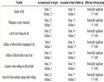
Table 1. Electronic parameters of the SnO2 thin films.
grain boundaries, the electronic state close to Fermi level is localized. When the states are localized, the conduction occurs by hopping of carriers between occupied and unoccupied localized which depends on the density of state and the position of Fermi level.
3.7. DC Conductivity (σdc)
The dc conductivity measurements of SnO2 thin films were carried out. The dc conductivity σdc of the SnO2 thin films was calculated using the relation;
 (20)
(20)
where, R is the measured resistance, t is the thickness of the films and A is the area of the films in contact with the electrode. The conductivity measurement was carried out at different temperatures ranging from 30˚C to 80˚C. From Figure 8, it can be seen that the dc conductivity was found to increase with increase in temperature. The plot indicates the exponential behavior of temperature dependent current confirming the semiconducting nature of the SnO2 thin films [19] . Traps which are present in the SnO2 thin films may be filled by excitation at low temperature and may be emptied by raising the temperature upon thermal activation. Upon thermal activation the mobility of charge carriers increases with a possible mechanism of hopping to cross the potential barrier and hence produce enhanced current. The value of activation energy was determined from the slope of lnσdc versus 1000/T (Figure 9) and it was found to be 0.28 eV.
3.8. Hall Measurements
The electrical properties of SnO2 films were studied by the Hall measurement using the van-der-Pauw method

Figure 8. Variation of dc conductivity versus temperature.

Figure 9. Plot of lnσdc versus 1000/T (K−1).
for the SnO2 films deposited on glass substrate to determine the carrier type, resistivity and mobility of the SnO2 films. Hall measurements were made at room temperature with a constant current (1 μA) and the magnetic field of 0.57 Tesla. The Hall mobility of the deposited SnO2 films was found to be 3.4 cm2/Vs. The resistivity, carrier concentration, and conductivity were (3.61 × 10⁻¹ Ωcm), (η = 5.4 × 10¹⁸ /cm3), and (0.0277 Ωcm) respectively.
4. Conclusion
The SnO2 thin films were prepared by using CBD technique. The XRD studies showed that the films prepared were in nanocrystalline range; also diffraction peaks were found. The size and the morphology of the SnO2 thin films were characterized by using SEM studies. The FT-IR spectrum exhibits the strong presence of SnO2. The band gap of SnO2 was found to be 3.5 eV. The optical constants such as refractive index, extinction coefficient and electrical susceptibility were calculated. The values of dielectric constant and dielectric loss were found to decrease with increase of frequency. In addition, the plasma energy of the valence electron, Penn gap or average energy gap, the Fermi energy, and electronic polarizability of SnO2 thin films were also determined. AC conductivity strongly depended on frequency and the conductivity was found to be increased at high frequencies. The activation energy was found to be 0.28 eV using dc electrical conductivity measurement. The Hall mobility of the material, resistivity, carrier concentration and conductivity were also estimated.
Cite this paper
SureshSagadevan,JibanPodder, (2015) Optical and Electrical Properties of Nanocrystalline SnO2 Thin Films Synthesized by Chemical Bath Deposition Method. Soft Nanoscience Letters,05,55-64. doi: 10.4236/snl.2015.54007
References
- 1. Lee, S., Kim, Y.W. and Chen, H. (2001) Electrical Properties of Ta-Doped Thin Films Prepared by the Metal-Organic Chemical-Vapor Deposition Method. Applied Physics Letters, 78, 350-352.
http://dx.doi.org/10.1063/1.1337640 - 2. Watson, J. (1984) The Tin Oxide Gas Sensor and Its Applications. Sensors and Actuators, 5, 29-42.
http://dx.doi.org/10.1016/0250-6874(84)87004-3 - 3. Minami, T. (1999) Transparent and Conductive Multicomponent Oxide Films Prepared by Magnetron Sputtering. Journal of Vacuum Science & Technology A, 17, 1765.
http://dx.doi.org/10.1116/1.581888 - 4. Liu, D., Wang, Q., Chang, H. and Chen, H. (1995) Variant Structure in Metal-Organic-Chemical-Vapor-Deposition-Derived SnO2 Thin Films on Sapphire (0001). Journal of Materials Research, 10, 1516-1522.
http://dx.doi.org/10.1557/JMR.1995.1516 - 5. Kaito, C. and Saito, Y. (1986) Structure and Crystallization Process of a Thin Film Prepared by Vacuum Evaporation of SnO2 Powder. Journal of Crystal Growth, 79, 403-409.
http://dx.doi.org/10.1016/0022-0248(86)90468-9 - 6. Lamelas, F. and Reid, S. (1999) Thin-Film Synthesis of the Orthorhombic Phase of SnO2. Physical Review B, 60, 9347.
http://dx.doi.org/10.1103/PhysRevB.60.9347 - 7. Choudhary, R., Ogale, S., Shinde, S., Kulkarni, V., Venkatesan, T., Harshavardhan, K., Strikovski, M. and Hannoyer, B. (2004) Pulsed-Electron-Beam Deposition of Transparent Conducting SnO2 Films and Study of Their Properties. Applied Physics Letters, 84, 1483.
http://dx.doi.org/10.1063/1.1651326 - 8. Ayouchi, R., Martin, F., Barrado, J., Martos, M., Morales, J. and Sánchez, L. (2000) Use of Amorphous Tin-Oxide Films Obtained by Spray Pyrolysis as Electrodes in Lithium Batteries. Journal of Power Sources, 87, 106-111.
http://dx.doi.org/10.1016/S0378-7753(99)00435-8 - 9. Baik, N., Sakai, G., Miura, N. and Yamazoe, N. (2000) Hydrothermally Treated Sol Solution of Tin Oxide for Thin-Film Gas Sensor. Sensors and Actuators B: Chemical, 63, 74-79.
http://dx.doi.org/10.1016/S0925-4005(99)00513-4 - 10. Ghoshtagor, R. (1978) Mechanism of CVD Thin Film SnO2 Formation. Journal of the Electrochemical Society, 125, 110-117.
http://dx.doi.org/10.1149/1.2131373 - 11. Deshpande, N., Vyas, J. and Sharma, R. (2008) Preparation and Characterization of Nanocrystalline Tin Oxide Thin Films Deposited at Room Temperature. Thin Solid Films, 516, 8587-8593.
http://dx.doi.org/10.1016/j.tsf.2008.06.016 - 12. Tsukuma, K., Akiyama, T. and Imai, H. (1997) Liquid Phase Deposition Film of Tin Oxide. Journal of Non-Crystalline Solids, 210, 48-54.
http://dx.doi.org/10.1016/S0022-3093(96)00583-2 - 13. Supothina, S. and De Guire, M. (2000) Characterization of SnO2 Thin Films Grown from Aqueous Solutions. Thin Solid Films, 371, 1-9.
http://dx.doi.org/10.1016/S0040-6090(00)00989-5 - 14. Ebrahimiasl, S., Yunus, W.Md.Z.W., Kassim, A. and Zainal, Z. (2011) Synthesis of Nanocrystalline SnOx (x = 1–2) Thin Film Using a Chemical Bath Deposition Method with Improved Deposition Time, Temperature and pH. Sensors, 11, 9207-9216.
http://dx.doi.org/10.3390/s111009207 - 15. Suresh, S. and Arunseshan, C. (2014) Dielectric Properties of Cadmium Selenide (CdSe) Nanoparticles Synthesized by Solvothermal Method. Applied Nanoscience, 4, 179-184.
http://dx.doi.org/10.1007/s13204-012-0186-5 - 16. Suresh, S. (2014) Studies on the Dielectric Properties of CdS Nanoparticles. Applied Nanoscience, 4, 325-329.
http://dx.doi.org/10.1007/s13204-013-0209-x - 17. Sagadevan, S. and Shanmuga Sundaram, A. (2014) Dielectric Properties of Lead Sulphide Thin films for Solar Cell Applications. Chalcogenide Letters, 11, 159-165.
- 18. Thirumavalavan, S., Mani, K. and Sagadevan, S. (2015) Structural, Surface Morphology, Optical And Electrical Investigation of CdSe Thin Films. Chalcogenide Letters, 12, 237-246.
- 19. Thirumavalavan, S., Mani, K. and Sagadevan, S. (2015) Investigation on Structural, Optical, Morphological and Electrical Properties of Lead Sulphide (PbS) Thin Films. Journal of Ovonic Research, 11, 123-130.
NOTES

*Corresponding author.