Applied Physics
Vol.1 No.1(2011), Article ID:66,11 pages DOI:10.4236/app.2011.11002
Research Progress in Nanophotonics Materials and Devices
Institute of Solid State Physics, Key Laboratory of Materials Physics, Chinese Academy of Sciences,
Anhui Key Laboratory of Nanomaterials and Nanotechnology, Hefei
Email: jxzhang@issp.ac.cn
Received: Mar. 23th, 2011; revised: Apr. 6th, 2011; accepted: Apr. 7th, 2011.
ABSTRACT:
The investigation field of nanophotonics is presented, this article provides a comprehensive review of research activities in nanophotonics materials and devices, and furthermore, the research progress of the materials and devices based on quantum confinement effect, light emission, surface plasmon polaritons (SPPs), and periodical structures is demonstrated significantly.
Keywords: Nanophotonics; Nanophotonics Materials; Nanophotonics Devices; Quantum Confinement; Light Emission; Surface Plasmon Polaritons; Photonic Crystal; Nanowire Grid Polarizers
纳米光子学材料与器件的研究进展
张俊喜*,张立德
中国科学院固体物理研究所,中国科学院材料物理重点实验室,
安徽省纳米材料与技术重点实验室,合肥
Email: jxzhang@issp.ac.cn
摘 要:
介绍了纳米光子学的研究范畴,综述了纳米光子学材料和器件的研究动态和热点,着重阐述了基于量子限域效应、光发射、表面等离子体激元和周期性结构纳米光子学材料和器件的研究进展。
收稿日期:2011年3月23日;修回日期:2011年4月6日;录用日期:2011年4月7日
关键词:纳米光子学;纳米光子学材料;纳米光子器件;量子限域;光发射;表面等离子体激元;光子晶体;纳米线栅偏振器
1. 引言
随着人类对信息永无止尽地追求,信息的传输和处理速度越来越快、数据存储密度越来越大已成为必然趋势。预计到2015年光纤传输系统的数据速率高达10 Tb/s,这就要求光子器件的尺度进一步减小并最终突破光的衍射极限而达到亚波长甚至纳米尺度。既然传统的光子器件对光的操纵受到光的半波长衍射极限的限制,因此探索光与物质在纳米尺度上相互作用的新原理、制备纳米光子学材料、构筑纳米光子器件以及发明纳米光子学制造技术将面临着新的挑战和机遇。
纳米光子学是研究在纳米尺度上光与物质相互作用的科学与技术,在纳米尺度上实现对光子的操纵和光学器件的构筑是纳米光子学的研究目标。纳米光子学不仅为研究在小于光波长的尺度上光与物质的相互作用过程提供富有挑战性的机遇,而且为纳米光子学材料在光子器件、纳米医学、纳米生物学等方面的应用创造了新的空间,同时为在更小尺度上的光学制造技术开辟了一条新的途径。人们对这种科学探索和技术发明的不断追求就是在逐步实现Richard P. Feynman的预言:“在下面尺度有大量的空间。”[1]作为一个新的前沿领域,纳米光子学已经引起了世界

Table 1. Category and content of nanophotonics
表1. 纳米光子学内容分类
范围内的广泛关注和极大兴趣。纳米光子学主要分为以下三个部分[2,3](表1)。
一是在纳米尺度上限制物质。在纳米尺度上构筑物质结构为控制材料的光学和电学性能提供了强有力的工具,已成为材料科学研究的前沿领域。通过选择不同类型的材料和控制材料的局域结构(如形貌和尺寸等)可以实现对光学性能的调控,不仅体现在线性光学而且在非线性光学中出现很多新奇的现象。例如,可以控制光学共振和局域场相互作用,通过控制局域声子态密度来操纵激发动力学以及通过控制结构之间的相互作用影响能量转换等。
二是在纳米尺度上限制波的辐射。传统光学研究的是光在远场空间的行为,由于光的衍射限制,所获得的光学信息是在宏观区域内的平均响应。近场扫描光谱(NSOM)和光子扫描隧道谱(PSTM)突破了光的衍射限制因而使得在纳米尺度上探测局域光场和研究近场区域光与物质相互作用成为可能。而且近场光学技术提供的高精度和高分辨将会在纳米光子学加工和制造中扮演重要角色,例如将锥形光纤探针涂上金属,光可以从远小于入射光波长的光纤探针尖端上发射而实现隧穿。
三是在纳米尺度上的光学加工。驱动未来工业应用需求的一系列光学加工技术越来越受到关注,包括集成电子线路,集成光电子耦合,表面处理,数据存储等。这些应用必然要求大幅度提高光学处理技术的精度和分辨率。传统光学加工器件的空间分辨依赖于光源的光斑尺寸而受到衍射极限的限制,而在纳米尺度上的光学加工不受这些限制而可以实现高精度和高分辨,同时可以为设计纳米光子结构和功能单元以及纳米结构器件提供一条行之有效的途径。
2. 基于量子限域效应的纳米光子学材料
由于半导体量子点的尺寸小于其激子波尔半径,所激发的电子与空穴的库仑相互作用很弱并形成各自能级,这使得半导体量子点有类似于原子分立能级的特征,因此可以产生窄线宽的荧光发射(线宽可以小于KBT)和高的荧光发射效率,从而显示出很强的量子限域效应。量子点的荧光可以通过单激发态[4-8]、双激发态[9,10]和多激发态[11,12]跃迁来实现。
既然尺寸分布不均匀会导致光发射谱加宽,要实现这种窄的荧光发射特性就需要制备尺寸分布均匀的高质量的量子点或单个量子点,目前的工作主要是围绕这方面展开的。如所制备的高质量直接带Ⅱ-Ⅵ族半导体量子点(CdSe[12-19], CdS[11], CdTe[20,21], CdSe/ZnSe[22], CdSe/ZnS[23]等)和Ⅲ-Ⅴ族(如InAs[4-6,24-27], InP[28,29], InAs/GaAs[30-32], InGaAs[33-35], InGaN[36], 和AlGaAs-GaAs[37]等)显示很高的荧光效率而可以作为很好的发光材料。另一方面,研究Si纳米结构的荧光性能主要集中在多孔硅[38,39]和硅纳米晶[40-42]上,而这些Si纳米结构的荧光发射带很宽。Sychugov等通过单个量子点荧光谱研究了从低温到室温单个Si纳米晶的发射线宽[43]。结果显示单个Si量子点在35 K显示了窄的发光(线宽为2 meV),至少可以达到直接带半导体量子点线宽,证实了强的量子限域效应。与多孔硅和Si纳米晶相比非晶硅(a-Si)本身的特点和a-Si量子点的量子限域效将期望在短波段作为很好的发光材料。Park等报道了采用PECVD的方法在SiN薄膜上制备高质量的a-Si量子点并在实验上首次证实了在零维a-Si中的量子限域效应导致强的荧光发射[44],而且通过控制量子点的尺寸可以调制

Figure 1. Exciton absorption spectrum of ordered PbSe nanowire arrays
图1. PbSe纳米线有序阵列的激子吸收谱
 (a) (b)
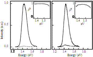
Figure 2. Excitation (a) and emission (b) spectra of an InP nanowire (the solid and the dashed lines correspond to the polarization directions of the exciting laser aligned parallel and perpendicular to the nanowire axis, respectively, inset, the spectra of the polarization ratio as a funcition of energy)
图2. 单根InP纳米线的激发谱(a)和发射谱(b)(实线和虚线分别为偏振方向平行和垂直于纳米线的谱图,插图是偏振度谱)
光发射波长(带隙从2.0 eV到2.76 eV)。由于量子点光发射的光沿各个方向传播,因而需要大的立体角的探测元件,这对光的探测器件提出了很高要求,那么针对这一难题可以通过调控发射光的传播方向来解决。最近Curto等设计了一种可以单方向传播的量子点光发射元件[45],是将单个量子点直接耦合到一种Yagi-Uda纳米天线上,这种通过在纳米天线的近场耦合产生的表面等离子体共振增加了光发射效率,而且量子点发射光具有很好的偏振性能和窄的发散角,其光发射方向性能够通过纳米天线的尺度进行控制。Bleuse等报道了将单个InAs量子点组装到GaAs量子线中实现对光发射的控制[46],这里量子线强烈地阻止自发光发射的连续辐射模式而产生一种有效的漏斗状的导光模式,即具有很好的方向性,这种复合结构有望作为一种单光子或纠缠光子对的高效量子光源。
和量子点类似,如果纳米线的直径小于激子波尔半径时也会产生量子限域效应。Korgel小组采用超流液相法制备了直径为4~5 nm的Si量子线并观察到由量子限域效应引起的可见波段的荧光发射[47],并在紫外到可见波段发现了窄的分立的光学跃迁以及强的带边荧光发射,这些光学特性主要来源于量子限域效应的贡献。最近Lansbergen等通过在p型Si纳米线构筑场效应晶体管通道中进行单个As原子掺杂实现对掺杂原子波函数的调制[48],通过晶体管栅极电势能够控制掺杂原子和邻近量子阱核势垒之间单电子掺杂态的杂化度,从而实现对单个掺杂原子的量子限域行为的控制。张立德小组报道了在氧化铝模板中组装PbSe纳米线[49],并观察到强的量子限域效应。由于PbSe的激子波尔半径为46 nm [50],这样就能在较大尺寸的PbSe中较容易的观察到强的量子限域效应。对部分去除氧化铝膜的PbSe纳米线阵列(纳米线直径为50 nm)的激子吸收谱研究显示从可见到紫外区存在两个很强、较宽的吸收峰(图1),位置分别在280 nm和434 nm 处,经分析研究发现位于280及434 nm处的峰分别来自于1se-1sh和1pe-1ph激子跃迁吸收。
3. 基于纳米线光发射的材料和器件
3.1. 偏振各向异性的发光材料
Lieber小组研究了单根InP纳米线室温下的光发射特性[51],发现当入射激光偏振方向从平行转变为垂直于纳米线轴向时荧光发射从开的状态转变为关的状态,显示了偏振各向异性的发射特性(图2)。他们预言了这种偏振敏感的半导体纳米线可以用在高密度光学元件之间的连接和光子线路中,同时有望在宽波段范围内包括光通信波长上作为高分辨探测器。
3.2. 纳米激光器
量子线或纳米线是研究尺寸对电子传输、光学性能调控的理想体系,可望作为纳米光子器件和光电子器件中的连接和功能元件。杨培东小组系统地研究了ZnO纳米线阵列的光发射特性并发现在室温下展示了紫外激光行为[52-54]。当激发功率低于激光阈值时显示的是一个自发发射的宽发射峰(半高宽为17 nm),这种光发射是由于激子复合产生的。随激发功率的增加,发射峰会变窄,当激发功率超过激光阈值(40 kW·cm-2)时,发射峰变得很窄(线宽小于0.3 nm)。这种ZnO纳米线阵列中观察到的激光行为表明并不需要制备单晶、像镜面端口的纳米线作为谐振腔。类似的激光发射在单根ZnO纳米线[55]、单根GaN纳米线[56]和InGaAs/GaAs异质结纳米柱[57]中也已经被观察到。
最近人们通过采用表面等离子体激元(SPPs)效应来限制纳米激光器光发射行为[58-60]。Noginov等设计了一种尺寸为44 nm的spaser激光器[59],这种激光器是采用Au纳米颗粒(核)/掺杂染料的氧化硅(壳)结构来实现,这种结构完全克服了SPPs在光学增益介质中的传输损耗,SPPs效应能够实现在一个纳米尺度的谐振腔中的光学频率共振而输出激光,这种spaser激光器是目前报道的在可见光波段(531 nm)最小的激光器。
3.3. 纳米发光二极管
Lieber小组采用构筑纳米线p-n结实现了二极管发光行为[61]。他们将p-型间接带隙半导体(如Si)纳米线和n-型直接带隙半导体(如CdS,CdSSe,CdSe和InP等)纳米线交叉连接构筑了纳米发光二极管(NanoLED),当加上高于带隙的偏压时n-型半导体纳米线单元会产生光发射而间接带隙Si纳米线是中性的。他们还将p-Si与n-GaN, CdS和CdSe交叉连接组装成多颜色NanoLED阵列(图3),发光峰位分别在365 nm,510 nm和690 nm,相应于GaN, CdS和CdSe的带边发射。这种交叉连接的NanoLED的发射颜色只受到直接带隙半导体的限制,而且器件有效面积为纳

Figure 3. Schematic image of a multicolor NanoLED array designed by p-Si/n-GaN, CdS, and CdSe nanowires
图3. p-Si和n-GaN, CdS和CdSe构筑的多颜色NanoLED阵列的示意图
米尺度因而可作为点光源,同时可以获得单一颜色和多重颜色,并可以实现光子和电子元件的集成。Taniyasu等设计了一种AlN紫外LED(波长在210 nm)[62],通过在AlN中的p型(Mg掺杂)和n型(Si掺杂)共掺杂获得p-AlN/AlN/n-AlN(AlN PIN)的同质结并可实现6 eV的宽直接带隙,其发光来自于激子跃迁,这是目前报道的最短波长的LED,有望用于高密度光存储和生物医学等领域。最近人们也采用有机聚合物(如PF-TAA和NRS-PPV)设计了从蓝光到橙色到红光的LED[63]。
4. 基于表面等离子体激元的光子学材料和器件
当物质结构的尺度减小到纳米尺度时,操纵光子将面临着突破光的衍射极限的困难,这使传统光学器件进一步小型化受到限制。激发表面等离子体激元(SPPs)有望给将来的光子器件开辟一条捷径。SPPs是一种沿着金属表面传播的电荷密度波,在光与金属表面自由电子相互作用时自由电子会在金属与电介质界面发生集体振荡而产生表面等离子体激元,进一步它与光场耦合会导致局域场增强。SPPs将在亚波长光学(如SPPs波导[64-71],SPPs光源[72-76])、近场光学[77-80]、表面增强光谱[81-85]、数据存储[86-88]、太阳能电池[89-91]、化学[92,93]和生物传感器[94-96]等方面有潜在的应用。
4.1. SPPs波导
Quinten等采用球形Ag纳米颗粒排列成线形链构筑亚波长光波导[64],其原理就是通过颗粒间的耦合作用实现光传输。当光只照射Ag纳米球链的最下端第一个颗粒时,发现偏振方向平行纳米球链轴时SPPs被激发,而且其它纳米球经耦合相继得到振动能量而使SPPs沿链传播;而偏振方向垂直纳米球链轴时SPPs波发生明显衰减。Weeber等报道了采用金属纳米线实现光的传播[66]。在电介质基底上淀积金属纳米线,线的短轴远小于入射光波长而线的长度大于光波长。采用某一波长的聚焦平面波照射纳米线的一端(entrance)时,在纳米线的另一端(exit)的近场区域出现了光场分布,这表明SPPs会沿纳米线传播。进一步结果表明在不同波长的入射光照射下,纳米线近场光强分布明显不同。采用633 nm的光照射时近场区只有照射点有光场,而用835 nm的光照射时发现在另一端近场区域有较强的光场(图4)。最近Oulton等将电介质圆柱纳米线用金属表面进行分隔[68],这种混杂结构可以在金属与电介质界面实现SPPs传输,这种混杂结构的SPPs波导具有强的局域性能够将光局限在l2/400~l2/40的范围内,而且能够实现低损耗、长距离传输(40~150 µm),通过调节结构参数可以将传输距离增加到毫米量级。要实现高的光数据传输速率需要将光学元件集成化,最近夏幼南小组实现了将多个Ag纳米线SPPs波导在聚合物光波导中的集成[69],这种光波导在一个芯片上能够用同一个聚合物波导将光耦合到多根金属纳米线中,而且通过改变入射光偏振来实现对耦合强度的控制。
除了采用纳米颗粒和纳米线设计SPPs波导以外,人们还采用多种形状的纳米通道实现SPPs的传输。
 (a)
(a) (b)
(b)
Figure 4. Distribution of the near-field electric intensity of nanowire for the incident wavelengths of 633 nm (a) and 835 nm (b)
图4. (a)和(b)分别为633 nm和835 nm波长光照射下纳米线近场区的光强分布
Ebbesen小组采用聚焦离子束(FIB)技术设计了V-型槽[70],Mach-Zehnder干涉仪和波导环共振器,这些结构可作为在光通信波长上的通道型传输模式的亚波长SPPs波导,这种波导具有强的SPPs局域行为和低的传输损耗。最近Nagpal等采用刻蚀方法制备不同构型的Si纳米图案(沟槽型、金字塔型、凸起型和孔型)[71],以此为模板组装相应形状的表面非常光滑的贵金属纳米结构并获得好方向性和低损耗的SPPs传输,而且实现器件的集成。
4.2. SPPs光源
Ebbesen小组通过采用聚焦离子束铣削方法制备亚波长周期性金属结构设计了SPPs光源[72]。图5(a)是在Ag薄膜上做一直径为250 nm的圆柱小孔,在小孔边缘刻有周期性同心圆沟槽,在出射端加工相同的结构。当光正入射到这些沟槽结构时表面会激发SPPs,SPPs通过小孔时产生透射增强效应,在沿小孔方向(0°)透射最强(图5(b)),显示经过出射端口时小孔
 (a)
(a) (b)
(b)
Figure 5. Pore structure with a periodical groove in an Ag film and the transmission intensity distribution with the collection angles, inset, schematic image of the incident and emergent beams
图5. (a)和(b)分别是小孔结构和相应的透射光强随探测角度的分布,插图是入射与出射光示意图
的光具有很好的方向性。
最近Oulton等在Ag薄膜衬底上设计了高光学增益的CdS纳米线[75],并将Ag薄膜衬底与CdS纳米线之间采用5 nm厚的MgF2绝缘层分隔,这种混杂结构能够将SPPs聚焦在金属与电介质界面的很小区域(l2/400),这比衍射极限光斑的尺寸小100倍,由于这种SPPs模式的高度局域性使得激光自发辐射率提高了六倍。朱星小组采用对称性破缺的Au纳米围栏实现对SPPs的亚波长单点聚焦,通过改变激发光的偏振行为和对称性破缺程度实现对SPPs干涉条纹的调制[76]。
4.3. 光存储
最近Zijlstra等报道了采用Au纳米棒的SPPs性质实现五维光存储[87]。由于Au纳米棒具有独特的光学和光热特性,窄的纵向表面等离子共振(LSPR)和偶极光学响应能够使得在激光照射区域内的少量纳米棒进行光学寻址,通过光热整形和双光子荧光探测来实现记录和读出。采用非线性双光子荧光探测具有好的角度和波长选择性,而单根纳米棒的散射和双光子荧光淬灭与波长和偏振有紧密的关系,在记录过程中,被选择的纳米棒吸收激光脉冲导致温度上升,对于足够高的激光脉冲能量,被选中的纳米棒的温度被加热到融化阈值以上,这时纳米棒的形状会被转换成短棒或球形颗粒,这会使得某一纵横比和取向的纳米棒数目减少,在荧光淬灭过程中产生了一个偏振影响的漂泊现象。采用Au作为记录媒介可以将波长、偏振和三个维度同时和在一起形成一个单独的五维存储技术,这种在同一记录体积中存储多个可单个寻址模式的复用存储技术能够大大提高光记录密度,记录密度可达到1 Tbit/cm3。
5. 基于周期性结构的纳米光子学材料和器件
5.1. 光子晶体
自从Yablonovitch[97]和John[98]各自提出了光子带隙的概念以来,近二十年光子带隙材料一直吸引了人们的关注,最近几年光子晶体仍然是研究热点。具有不同介电常数的介质材料按周期性排列,在其中传播的光波的色散曲线将成为带状结构,带与带之间会出现类似于半导体带隙的光子带隙,频率落在带隙中的光波被严格禁止传播,这种具有光子带隙的周期性电介质结构称为光子晶体,它可分为一维、二维和三维光子晶体。
光子晶体为光学器件的小型化和集成化创造了史无前例的机遇,这归因于它新的物理特性如抑制和增强光的自发发射,具有低的激光阈值,和量子信息处理等。研究较多的是红外波段的光子晶体[99-103],可见[104-107]和紫外[108]波段上的光子带隙材料也开始崭露头角。在二维光子晶体的一个重要进展就是采用周期性孔阵列设计光子晶体光纤[109,110],与传统光纤相比这种光纤可以实现低的光损耗。最近Noda小组在芯片上设计了一种二维方形和矩形格子的光子晶体激光器[111],通过改变格子的参数实现对激光共振条件和输出光束方向的控制,而且通过动力学控制芯片集成化的连续扫描能够使得输出激光的光束在一定方向范围内(相对于入射光方向最大偏离角度可达30°)调制。Tandaechanurat等报道了在GaAs基的二维薄层中堆垛三层高密度的InAs量子点构筑一种三维光子晶体[112],实现了在三维光子晶体谐振腔中的光子振荡,输出的激光由于量子点耦合谐振腔共振模式而获得了很高的激光品质因子(Q因子约38500),这种将激光模式局域在三维光子晶体的完全光子带隙中能强烈地限制光子在谐振腔中并有效地阻止自发光发射。
要实现光子晶体的应用需要解决以下几个问题:一是在光波段构筑完全光子带隙的三维光子晶体;二是将任意缺陷态引入到光子晶体中;三是引入一种有效的光发射元件。制备三维光子晶体的有很多方法,例如熔化粘结和激光束辅助排列技术[102,113]、自组装方法[114-117]、微机械硅加工技术[118]、掠射角淀积技术[119]和蚀刻技术[101,104,120-122]等。
5.2. 纳米线栅偏振器
光偏振在光隔离、光调制、光开关等光学元件中扮演重要角色。在许多光学元件和光电子元件中,必不可少的是要由偏振器来产生或检验线偏振光。偏振器的偏振性能如何将直接影响到这些元件的性能。随着光学技术的飞速发展,偏振器的微型化和高性能将成为必然趋势,其中线栅偏振器便于实现微型化,它会在将来的光通讯、集成光学、光电探测中有重要的应用前景。
线栅偏振器通常采用蒸发和刻蚀技术设计。Bird等采用掠入射方法在熟料光栅复型基底上通过蒸发金属来制备线栅偏振器[123],这种线栅的周期是463 nm,它在2~15 µm的红外波段显示偏振现象。Young等采用不同衬底材料(如ZnS和ZnSe)来改进线栅的偏振性能[124],它适用于6~20 µm的红外波段。Doumuki等利用电子束刻蚀技术成功地在SiO2[125]和GaAs[126]衬底上制备了Al线栅微偏振器,其中在SiO2基底上制备的Al线栅周期为390 nm,由于s偏振共振效应而在近红外波长显示了偏振现象。2005年,Wang等采用纳米印章刻蚀和电子束蒸发相结合的方法制备了高性能纳米线栅偏振器[127],首先通过纳米印章刻蚀技术构筑电介质(如SiO2)纳米壁,然后采用电子束蒸发在纳米壁侧面和底部沉积Au膜形成线栅芯结构,纳米壁宽和高分别为60 nm和515 nm,侧面和顶部的Au膜厚度为24 nm,光学测量结果显示这种纳米线栅在近红外波段(C带)消光比可以达到40 dB而在整个C带透射率可达97%。最近Lin等采用刻蚀技术在光纤上制备了一种宽波段范围的Au线栅偏振器[128],线栅周期为200 nm,线栅厚度为100 nm, 在1310 nm和1550 nm通信波长的消光比分别达到15.6 dB和20.5 dB。
以上都是采用自上而下(Top-down)的方法设计线栅偏振器,其优势是在近红外到中红外波段展示较好的偏振性能,而且在器件连接和光学测量上可操作性强,它的不足是制备过程复杂且技术昂贵,且线尺寸很难达到纳米尺度;相比较而言,采用自下而上(Bottom-up)的方法也可以设计线栅偏振器,这种方法具有成本低、制备过程简单、可控性好、容易实现小型化。
张立德小组报道了采用金属纳米线有序阵列可以设计在可见到近红外波段上的线栅偏振器,对单一尺寸的金属纳米线阵列的光偏振研究表明金属纳米线阵列在该波段显示了较好的偏振性能[129,130]。
张俊喜对金属纳米线阵列产生光偏振的机理进行深入研究,分析结果表明消光比来自于界面Fresnel反射和金属纳米线的吸收而插入损耗是源于金属纳米线Rayleigh散射的贡献。采用氧化铝模板技术构筑的金属纳米线阵列可以将线栅周期降低到纳米尺度,因而通过优化尺度参数能够将金属纳米线阵列用于构筑一种新型的线栅偏振器(图6),我们称之为纳米线栅偏振器,这是国际上最早提出纳米线栅偏振器概念的报道(2004年)[131]。在此基础上,我们系统研究了金属纳米线尺度对偏振性能的调制,结果表明纳米线的直径和间距对消光比和插入损耗具有同步的调制行为[131](图7,图8),随直径增加消光比提高但插入损耗也增大了,另一方面随间距增加插入损耗降低但消光比也减小了。
将纳米线的直径与间距同时考虑,在此基础上我们发现一个影响偏振性能的重要参数:直径与间距之比[132]。系统研究了这一参数对消光比与插入损耗的影响并进行合理的解释,由此提出基于金属纳米线阵列构筑纳米线栅偏振器的优化设计方案既通过选择适中的直径与间距的比值不变然后减小直径,从而同时获得最高的消光比和最低的插入损耗(图9)。我们设计的基于金属纳米线阵列构筑纳米线栅偏振器的期望值:在光通信的1550 nm波长消光比为40 dB,而插入损耗为0.5 dB,而在大于这一通信波长消光比大于40 dB而插入损耗小于0.5 dB。

Figure 6. Schematic image of nanowire grid polarizer designed by a metal nanowire microarray
图6. 金属纳米线阵列构筑纳米线栅偏振器的结构示意图

Figure 7. The optical loss spectra of the microarrays of copper nanowires with uniform spacing of 130 nm but different diameters of 30 nm, 65 nm, and 100 nm, where, Ls and Lp are the extinction ratio and the insertion loss, respectively
图7. 相同间距(130 nm)、不同直径(30, 65, 100 nm)的Cu纳米线阵列的光学损耗谱,其中Ls为消光比,Lp为插入损耗

Figure 8. The optical loss spectra of the microarrays of copper nanowires with uniform diameter of 50 nm but different spacing of 70 nm, 100 nm, and 130 nm
图8. 相同直径(50 nm)、不同间距(70 nm, 100 nm, 130 nm)的Cu纳米线阵列的光学损耗谱

Figure 9. Diameter evolution of optical loss spectra of the microarrays of silver nanowires when selecting the ratio of 2a and b of 0.5
图9. 当2a/b为0.5时不同直径的Ag纳米线阵列的光学损耗谱
6. 小结与展望
本文综述了纳米光子学材料和器件的研究进展,着重从以下几个方面介绍:一是基于量子限域效应的纳米光子学材料,包括Ⅱ-Ⅵ和Ⅲ-Ⅴ族半导体量子点,Si量子点和量子线,以及PbSe量子线,这些纳米光子学材料显示出强的量子限域效应,具有高的荧光发射效率;二是基于纳米线光发射的材料与器件,包括具有偏振各向异性光发射的InP纳米线,具有窄的紫外光发射可作为纳米激光器的ZnO纳米线阵列,采用间接带隙和直接带隙交叉连接构筑紫外到近红外波长的纳米发光二极管(NanoLED);三是基于SPPs的光子学材料和器件,包括贵金属纳米颗粒和纳米线SPPs波导,周期性结构诱导的局域场增强并实现SPPs聚焦而构筑SPPs光源,以及由于SPPs效应实现五维光存储贵金属纳米棒材料等;四是基于周期性结构的纳米光子学材料和器件,包括采用周期性电解质设计的红外、可见甚至到紫外波段的光子晶体,采用金属纳米线阵列设计高性能的纳米线栅偏振器等。纳米光子学的进一步发展面临很多挑战,譬如,发展纳米技术如何实现更小、高效、高稳定性的纳米光子器件,如何实现全光集成化,发展新材料、新原理和新技术如何调控纳米光子学材料和器件的性能并实现性能优化,如何将纳米光子学材料和纳米光子器件的应用加以拓宽,不仅局限在光子学领域而且利用纳米光子学的特点能够有效地应用到环境、能源、生物、医药和健康等领域。
7. 致谢
感谢国家自然科学基金(10804112)和973项目(2007CB936601)的资助。
参考文献 (References)
[1] R. P. Feynman. There’s plenty of room at the bottom—an invitation to enter a new field of physics[EB/OL]. http://www.zyvex.com/nanotech/feynman.html
[2] Y. Z. Shen, C. S. Friend, Y. Jiang, et al. Nanophotonics: interactions, materials, and applications. J. Phys. Chem. B, 2000, 104(32): 7577-7587.
[3] Y. Shen, P. N. Prasad. Nanophotonics: a new multidisciplinary frontier.Applied Physics B: Lasers and Optics, 2002, 74(7-8): 641-645.
[4] P. Michler, A. Kiraz, C. Becher, et al. A quantum dot single-photon turnstile device. Science, 2000, 290(5500): 2282- 2285.
[5] C. Santori, D. Fattal, J. Vučković, et al. Indistinguishable photons from a single-photon device. Nature, 2002, 419(6907): 594- 597.
[6] Z. L. Yuan, B. E. Kardynal, R. M. Stevenson, et al. Electrically driven single-photon source. Science, 2002, 295(5552): 102- 105.
[7] F. Sotier, T. Thomay, T. Hanke, et al. Femtosecond few-fermion dynamics and deterministic single-photon gain in a quantum dot. Nat. Phys., 2009, 5(5): 352-356.
[8] S. Kako, C. Santori, K. Hoshino, et al. A gallium-nitride single-photon source operating at 200 K. Nat. Mater., 2006, 5(11): 887-892.
[9] X. Q. Li, Y. W. Wu, D. C. Steel, et al. An all-optical quantum gate in a semiconductor quantum dot. Science, 2003, 301(5634): 809-811.
[10] R. B. Patel, A. J. Bennett, I. Farrer, et al. Two-photon interference of the emission from electrically tunable remote quantum dots. Nat. Photonics, 2010, 4(9): 632-635.
[11] J. R. Lakowicz, I. Gryczynski, G. Piszczek, et al. Emission spectral properties of cadmium sulfide nanoparticles with multiphoton Excitation. J. Phys. Chem. B, 2002, 106(21): 5365 -5370.
[12] B. Fisher, J. M. Caruge, D. Zehnder, et al. Room-temperature ordered photon emission from multiexciton states in single CdSe core-shell nanocrystals. Phys. Rev. Lett., 2005, 94(8), p.087403.
[13] S. A. Empedocles, D. J. Norris, M. G. Bawendi. Photoluminescence spectroscopy of single CdSe nanocrystallite quantum dots. Phys. Rev. Lett., 1996, 77(18): 3873-3876.
[14] S. A. Empedocles, M. G. Bawendi. Quantum-confined stark effect in single CdSe nanocrystallite quantum dots. Science, 1997, 278(5346): 2114-2117.
[15] V. I. Klimov, A. A. Mikhailovsky, S. Xu, et al. Optical gain and stimulated emission in nanocrystal quantum dots. Science, 2000, 290(5490): 314-317.
[16] X. Y. Wang, L. H. Qu, J. Y. Zhang, et al. Surface-related emission in highly luminescent CdSe quantum dots. Nano Lett., 2003, 3(8): 1103-1106.
[17] D. Pacifici, H. J. Lezec, H. A. Atwater. All-optical modulation by plasmonic excitation of CdSe quantum dots. Nat. Photonics, 2007, 1(7): 402-406.
[18] A. V. Akimov, A. Mukherjee, C. L. Yu, et al. Generation of single optical plasmons in metallic nanowires coupled to quantum dots. Nature, 2007, 450(7168): 402-406.
[19] R. Beaulac, L. Schneider, P. I. Archer, et al. Light-induced spontaneous magnetization in doped colloidal quantum dots. Science, 2009, 325(5943): 973-976.
[20] Z. Y. Tang, N. A. Kotov, M. Giersig. Spontaneous organization of single CdTe nanoparticles into luminescent nanowires. Science, 2002, 297(5579): 237-240.
[21] J. Y. Zhang, X. Y. Wang, M. Xiao, et al. Modified spontaneous emission of CdTe quantum dots inside a photonic crystal. Opt. Lett., 2003, 28(16): 1430-1432.
[22] V. D. Kulakovskii, G. Bacher, R. Weigand, et al. Fine structure of biexciton emission in symmetric and symmetric CdSe/ZnSe single quantum dots. Phys. Rev. Lett., 1999, 82(8): 1780-1783.
[23] Q. Sun, Y. A. Wang, L. S. Li, et al. Bright, multicoloured light-emitting diodes based on quantum dots. Nat. Photonics, 2007, 1(11): 717-722.
[24] G. S. Solomon, M. Pelton, Y. Yamamoto. Single-mode spontaneous emission from a single quantum dot in a three-dimensional microcavity. Phys. Rev. Lett., 2001, 86(17): 3903-3906.
[25] E. Moreau, I. Robert, L. Manin, et al. Quantum cascade of photons in semiconductor quantum dots. Phys. Rev. Lett., 2001, 87(18), p.183601.
[26] S. Kan, T. Mokari, E. Rothenberg, et al. Synthesis and size-dependent properties of zinc-blende semiconductor quantum rods. Nat. Mater., 2003, 2(2): 155-158.
[27] E. A. Stinaff, M. Scheibner, A. S. Bracker, et al. Optical signatures of coupled quantum dots. Science, 2006, 311(5761): 636-639.
[28] O. I. Mićić, J. Sprague, Z. H. Lu, et al. Highly efficient band-edge emission from InP quantum dots. Appl. Phys. Lett., 1996, 68(22): 3150-3152.
[29] H. X. Fu, A. Zunger. InP quantum dots: electronic structure, surface effects, and the redshifted emission. Phys. Rev. B, 1997, 56(3): 1496-1508.
[30] L. Harris, D. J. Mowbray, M. S. Skolnick, et al. Emission spectra and mode structure of InAs/GaAs self-organized quantum dot lasers. Appl. Phys. Lett., 1998, 73(7): 969-971.
[31] W. Fang, J. Y. Xu, A. Yamilov, et al. Large enhancement of spontaneous emission rates of InAs quantum dots in GaAs microdisks. Opt. Lett., 2002, 27(11): 948-950.
[32] E. S. Moskalenko, F. K. Karlsson, V. T. Donchev, et al. Effects of separate carrier generation on the emission properties of InAs/GaAs quantum dots. Nano Lett., 2005, 5(11): 2117-2122.
[33] P. Borri, W. Langbein, S. Schneider, et al. Ultralong dephasing time in InGaAs quantum dots. Phys. Rev. Lett., 2001, 87(15), p. 157401.
[34] H. Kamada, H. Gotoh, J. Temmyo, et al. Exciton Rabi oscillation in a single quantum dot. Phys. Rev. Lett., 2001, 87(24), p. 246401.
[35] A. Högele, S. Seidl, M. Kroner, et al. Voltage -controlled optics of a quantum dot. Phys. Rev. Lett., 2004, 93(21), p.217401.
[36] Y. Narukawa, Y. Kawakami, M. Funato, et al. Role of self-formed InGaN quantum dots for exciton localization in the purple laser diode emitting at 420 nm. Appl. Phys. Lett., 1997, 70(8): 981-983.
[37] T. Fujisawa, T. H. Oosterkamp, W. G. van der Wiel, et al. Spontaneous emission spectrum in double quantum dot devices. Science, 1998, 282(5390): 932-935.
[38] D. Kovalev, H. Heckler, B. Averboukh, et al, Hole burning spectroscopy of porous silicon. Phys. Rev. B, 1998, 57(7): 3741-3744.
[39] M. Cazzanelli, D. Kovalev, L. D. Negro, et al. Polarized optical gain and polarization-narrowing of heavily oxidized porous silicon. Phys. Rev. Lett., 2004, 93(20), p. 207402.
[40] D. Kovalev, H. Heckler, M. Ben-Chorin, et al. Breakdown of the k-conservation rule in Si nanocrystals. Phys. Rev. Lett., 1998, 81(13): 2803-2806.
[41] L. Bagolini, A. Mattoni, G. Fugallo, et al. Quantum confinement by an order-disorder boundary in nanocrystalline silicon. Phys. Rev. Lett., 2010, 104(17), p.176803.
[42] M. Fuechsle, S. Mahapatra, F. A. Zwanenburg, et al. Spectroscopy of few-electron single-crystal silicon quantum dots. Nat. Nanotechnol., 2010, 5(7): 502-505.
[43] I. Sychugov, R. Juhasz, J. Valenta, et al. Narrow luminescence linewidth of a silicon quantum dot. Phys. Rev. Lett., 2005, 94(8), p. 087405.
[44] N. M. Park, C. J. Choi, T. Y. Seong, et al. Quantum confinement in amorphous silicon quantum dots embedded in silicon nitride. Phys. Rev. Lett., 2001, 86(7): 1355-1357.
[45] A. G. Curto, G. Volpe, T. H. Taminiau, et al. Unidirectional emission of a quantum dot coupled to a nanoantenna. Science, 2010, 329(5994): 930-933.
[46] J. Bleuse, J. Claudon, M. Creasey, et al. Inhibition, enhancement, and control of spontaneous emission in photonic nanowires. Phys. Rev. Lett., 2011, 106(10), p.103601.
[47] J. D. Holmes, K. P. Johnston, R. C. Doty, et al. Control of thickness and orientation of solution-grown silicon nanowires. Science, 2000, 287(5457): 1471-1473.
[48] G. P. Lansbergen, R. Rahman, C. J. Wellard, et al. Gate-induced quantum-confinement transition of a single dopant atom in a silicon FinFET. Nat. Phys., 2008, 4(8): 656-661.
[49] X. S. Peng, G. W. Meng, J. Zhang, et al. Strong quantum confinement in ordered PbSe nanowire arrays. Journal of Materials Research, 2002, 17(6): 1283-1286.
[50] F. W. Wise. Lead salt quantum dots: the limit of strong quantum confinement. Acc. Chem. Res., 2000, 33(11): 773-780.
[51] J. F. Wang, M. S. Gudiksen, X. F. Duan, et al. Highly polarized photoluminescence and photodetection from single indium phosphide nanowires. Science, 2001, 293(5534): 1455-1457.
[52] M. H. Huang, S. Mao, H. Feick, et al. Room-temperature ultraviolet nanowire nanolasers. Science, 2001, 292(5523): 1897- 1899.
[53] P. D. Yang, H. Q. Yan, S. Mao, et al. Controlled growth of ZnO nanowires and their optical properties. Adv. Funct. Mater., 2002, 12(5): 323-331.
[54] H. Q. Yan, R. R. He, J. Johnson, et al. Dendritic nanowire ultraviolet laser array. J. Am. Chem. Soc., 2003, 125(16): 4728-4729.
[55] J. C. Johnson, H. Q. Yan, R. D. Schaller, et al. Single nanowire lasers. J. Phys. Chem. B, 2001, 105(46): 11387-11390.
[56] J. C. Johnson, H. J. Choi, K. P. Knutsen, et al. Single gallium nitride nanowire lasers. Nat. Mater., 2002, 1(2): 106-110.
[57] R. Chen, T. T. D. Tran, K. W. Ng, et al. Nanolasers grown on silicon. Nat. Photonics, 2011, 5(3): 170-175.
[58] N. F. Yu, J. Fan, Q. J. Wang, et al. Small-divergence semiconductor lasers by plasmonic collimation. Nat. Photonics, 2008, 2(7): 564-570.
[59] M. A. Noginov, G. Zhu, A. M. Belgrave, et al. Demonstration of a spaser-based nanolaser. Nature, 2009, 460(7259): 1110-1112.
[60] R. F. Service. Ever-smaller lasers pave the way for data highways made of light. Science, 2010, 328(5980): 810-811.
[61] Y. Huang, X. F. Duan, C. M. Lieber. Nanowires for integrated multicolor nanophotonics. Small, 2005, 1(1): 142-147.
[62] Y. Taniyasu, M. Kasu, T. Makimoto. An aluminium nitride light-emitting diode with a wavelength of 210 nanometres. Nature, 2006, 441(7091): 325-328.
[63] S. L. M. van Mensfoort, M. Carvelli, M. Megens, et al. Measuring the light emission profile in organic light-emitting diodes with nanometre spatial resolution. Nat. Photonics, 2010, 4(3): 329-335.
[64] M. Quinten, A. Leitner, J. R. Krenn, et al. Electromagnetic energy transport via linear chains of silver nanoparticles. Opt. Lett., 1998, 23(17): 133-1333.
[65] S. A. Maier, P. G. Kik, H. A. Atwater, et al. Local detection of electromagnetic energy transport below the diffraction limit in metal nanoparticle plasmon waveguides. Nat. Mater., 2003, 2(4): 229-232.
[66] J. C. Weeber, A. Dereux, C. Girard, et al. Plasmon polaritons of metallic nanowires for controlling submicron propagation of light. Phys. Rev. B, 1999, 60(12): 9061-9068.
[67] S. I. Bozhevolnyi, J. Erland, K. Leosson, et al. Waveguiding in surface plasmon polariton band gap structures. Phys. Rev. Lett., 2001, 86(14): 3008-3011.
[68] R. F. Oulton, V. J. Sorger, D. A. Genov, et al. A hybrid plasmonic waveguide for subwavelength confinement and long range propagation. Nat. Photonics, 2008, 2(8): 496-500.
[69] A. L. Pyayt, B. Wiley, Y. N. Xia, et al. Integration of photonic and silver nanowire plasmonic waveguides. Nat. Nanotechnol., 2008, 3(10): 660-665.
[70] S. I. Bozhevolnyi, V. S. Volkov, E. Devaux, et al. Channel plasmon subwavelength waveguide components including interferometers and ring resonators. Nature, 2006, 440(7083): 508-511.
[71] P. Nagpal, N. C. Lindquist, S. H. Oh, et al. Ultrasmooth patterned metals for plasmonics and metamaterials. Science, 2009, 325(5940): 594-597.
[72] H. J. Lezec, A. Degiron, E. Devaux, et al. Beaming light from a subwavelength aperture. Science, 2002, 297(5582): 820-822.
[73] G. Lerosey, D. F. P. Pile, P. Matheu, et al. Controlling the phase and amplitude of plasmon sources at a subwavelength scale. Nano Lett., 2009, 9(1): 327-331.
[74] A. F. Koenderink. Plasmon nanoparticle array waveguides for single photon and single plasmon sources. Nano Lett., 2009, 9(12): 4228-4233.
[75] R. F. Oulton, V. J. Sorger, T. Zentgraf, et al. Plasmon lasers at deep subwavelength scale. Nature, 2009, 461(7264): 629-632.
[76] Z. Y. Fang, Q. A. Peng, W. T. Song, et al. Plasmonic focusing in symmetry broken nanocorrals. Nano Lett., 2011, 11(2): 893-897.
[77] M. Achermann, K. L. Shuford, G. C. Schatz, et al. Near-field spectroscopy of surface plasmons in flat gold nanoparticles. Opt. Lett., 2007, 32(15): 2254-2256.
[78] S. Kim, J. H. Jin, Y. J. Kim, et al. High-harmonic generation by resonant plasmon field enhancement. Nature, 2008, 453(7196): 757-760.
[79] M. Schnell, A. Garcia-Etxarri, A. J. Huber, et al. Controlling the near-field oscillations of loaded plasmonic nanoantennas. Nat. Photonics, 2009, 3(4): 287-291.
[80] S. Kawata, Y. Inouye, P. Verma. Plasmonics for near-field nano-imaging and superlensing. Nature Photonics, 2009, 3(7): 388-394.
[81] A. C. R. Pipino, R. P. VanDuyne, G. C. Schatz. Surface -enhanced second-harmonic diffraction: Experimental investigation of selective enhancement. Phys. Rev. B, 1996, 53(7): 4162-4169.
[82] S. M. Nie, S. R. Emery. Probing single molecules and single nanoparticles by surface-enhanced Raman scattering. Science, 1997, 275(5303): 1102-1106.
[83] Y. Fang, N. H. Seong, D. D. Dlott. Measurement of the distribution of site enhancements in surface-enhanced Raman scattering. Science, 2008, 321(5887): 388-392.
[84] A. Gopinath, S. V. Boriskina, W. R. Premasiri, et al. Plasmonic nanogalaxies: multiscale aperiodic arrays for surface-enhanced raman sensing. Nano Lett., 2009, 9(11): 3922-3929.
[85] Y. R. Fang, H. Wei, F. Hao, et al. Remote-excitation surfaceenhanced raman scattering using propagating Ag nanowire plasmons. Nano Lett., 2009, 9(5): 2049-2053.
[86] C. Hermann, V. A. Kosobukin, G. Lampel, et al. Surface-enhanced magneto-optics in metallic multilayer films. Phys. Rev. B, 2001, 64(23), p. 235422.
[87] P. Zijlstra, J. W. M. Chon, M. Gu. Five-dimensional optical recording mediated by surface plasmons in gold nanorods. Nature, 2009, 459(7245): 410-413.
[88] D. O'Connor, A. V. Zayats. Data storage: the third plasmonic revolution. Nat. Nanotechnol., 2010, 5(7): 482-483.
[89] M. Westphalen, U. Kreibig, J. Rostalski, et al. Metal cluster enhanced organic solar cells. Sol. Energ. Mat. Sol. C, 2000, 61(1): 97-105.
[90] V. E. Ferry, L. A. Sweatlock, D. Pacifici, et al. Plasmonic nanostructure design for efficient light coupling into solar cells. Nano Lett., 2008, 8(12): 4391-4397.
[91] M. D. Brown, T. Suteewong, R. S. S. Kumar, et al. Plasmonic dye-sensitized solar cells using core-shell metal-insulator nanoparticles. Nano Lett., 2011,11(2): 438-445.
[92] F. Goettmann, A. Moores, C. Boissière, et al. A selective chemical sensor based on the plasmonic response of phosphinine-stabilized gold nanoparticles hosted on periodically organized mesoporous silica thin layers. Small, 2005, 1(6): 636-639.
[93] J. Homola, S. S. Yee, G. Gauglitz. Surface plasmon resonance sensors: review. Sensors Actuat. B, 1999, 54(1-2): 3-15.
[94] S. J. Chen, F. C. Chien, G. Y. Lin, et al. Enhancement of the resolution of surface plasmon resonance biosensors by control of the size and distribution of nanoparticles. Opt. Lett., 2004, 29(12): 1390-1392.
[95] J. N. Anker, W. P. Hall, O. Lyandres, et al. Biosensing with plasmonic nanosensors. Nat. Mater., 2008, 7(6): 442-453.
[96] A. V. Kabashin, P. Evans, S. Pastkovsky, et al. Plasmonic nanorod metamaterials for biosensing. Nat. Mater., 2009, 8(11): 867-871.
[97] E. Yablonovitch. Inhibited spontaneous emission in solid-state physics and electronics. Phys. Rev. Lett., 1987, 58(20): 2059- 2062.
[98] S. John. Strong localization of photons in certain disordered dielectric superlattices. Phys. Rev. Lett., 1987, 58(23): 2486- 2489.
[99] O. Painter, R. K. Lee, A. Scherer, et al. Two-dimensional photonic band-gap defect mode laser. Science, 1999, 284(5421): 1819-1821.
[100] S. Inoue1, Y. Aoyagi. Design and fabrication of two-dimensional photonic crystals with predetermined nonlinear optical properties. Phys. Rev. Lett., 2005, 94(10), p. 103904.
[101] S. Y. Lin, J. G. Fleming, D. L. Hetherington, et al. A three-dimensional photonic crystal operating at infrared wavelengths. Nature, 1998, 394(6690): 251-253.
[102] E. Chow, S. Y. Lin, S. G. Johnson, et al. Three-dimensional control of light in a two-dimensional photonic crystal slab. Nature, 2000, 407(6807): 983-986.
[103] S. Noda, K. Tomoda, N. Yamamoto, et al. Full three-dimensional photonic bandgap crystals at near-infrared wavelengths. Science, 2000, 289(5479): 604-606.
[104] J. G. Fleming, S. Y. Lin, I. El-Kady, et al, All-metallic three-dimensional photonic crystals with a large infrared bandgap. Nature, 2002, 417(6884): 52-55.
[105] M. Campbell, D. N. Sharp, M. T. Harrison, et al. Fabrication of photonic crystals for the visible spectrum by holographic lithography. Nature, 2000, 404(6773): 53-56.
[106] H. Matsubara, S. Yoshimoto, H. Saito, et al. GaN photoniccrystal surface-emitting laser at blue-violet wavelengths. Science, 2008, 319(5862): 445-447.
[107] B. Corcoran, C. Monat, C. Grillet, et al. Green light emission in silicon through slow-light enhanced third-harmonic generation in photonic-crystal waveguides. Nat. Photonics, 2009, 3(4): 206- 210.
[108] A. Yamilov, X. Wu, X. Liu, et al. Self-optimization of optical confinement in an ultraviolet photonic crystal slab laser. Phys. Rev. Lett., 2006, 96(8), p.083905.
[109] J. C. Knight. Photonic crystal fibres. Nature, 2003, 424(6950): 847-851.
[110] R. F. Cregan, B. J. Mangan, J. C. Knight, et al. Single-mode photonic band gap guidance of light in air. Science, 1999, 285(5433): 1537-1539.
[111] Y. Kurosaka, S. Iwahashi, Y. Liang, et al. On-chip beam-steering photonic-crystal lasers. Nat. Photonics, 2010, 4(7): 447-450.
[112] A. Tandaechanurat, S. Ishida, D. Guimard, et al. Lasing oscillation in a three-dimensional photonic crystal nanocavity with a complete bandgap. Nat. Photonics, 2011, 5(2): 91-94.
[113] S. Ogawa, M. Imada, S. Yoshimoto, et al. Control of light emission by 3D photonic crystals. Science, 2004, 305(5681): 227- 229.
[114] J. E. G. J. Wijnhoven, W. L. Vos. Preparation of photonic crystals made of air spheres in titania. Science, 1998, 281(5378): 802-804.
[115] P. V. Braun, P. Wiltzius. Microporous materials: Electrochemically grown photonic crystals. Nature, 1999, 402(6762): 603-604.
[116] A. Blanco, E. Chomski, S. Grabtchak, et al. Large-scale synthesis of a silicon photonic crystal with a complete threedimensional bandgap near 1.5 micrometres. Nature, 2000, 405(6785): 437-440.
[117] Y. A. Vlasov, X. Z. Bo, J. C. Sturm, et al. On-chip natural assembly of silicon photonic bandgap crystals. Nature, 2001, 414(6861): 289-293.
[118] J. G. Fleming, S. Y. Lin. Three-dimensional photonic crystal with a stop band from 1.35 to 1.95 mm. Opt. Lett., 1999, 24(1): 49-51.
[119] O. Toader, S. John. Proposed square spiral microfabrication architecture for large three-dimensional photonic band gap crystals. Science, 2001, 292(5519): 1133-1135.
[120] M. H. Qi, E. Lidorikis, P. T. Rakich, et al. A three-dimensional optical photonic crystal with designed point defects. Nature, 2004, 429(6991): 538-542.
[121] S. Takahashi, K. Suzuki, M. Okano, et al. Direct creation of three-dimensional photonic crystals by a top-down approach. Nat. Mater., 2009, 8(9): 721-725.
[122] K. Ishizaki, S. Noda. Manipulation of photons at the surface of three-dimensional photonic crystals. Nature, 2009, 460(7253): 367-370.
[123] G. R. Bird, M. Parrish. The wire grid as a near-infrared polarizer. J. Opt. Soc. Am., 1960, 50(9): 886-891.
[124] J. B. Young, H. A. Graham, E. W. Peterson. Wire grid infrared polarizer. Appl. Opt., 1965, 4(8): 1023-1026.
[125] H. Tamada, T. Doumuki, T. Yamaguchi, et al. Al wire-grid polarizer using the s-polarization resonance effect at the 0.8-mm-wavelength band. Opt. Lett., 1997, 22(6): 419-421.
[126] T. Doumuki, H. Tamada. An aluminum-wire grid polarizer fabricated on a gallium-arsenide photodiode. Appl. Phys. Lett., 1997, 71(5): 686-688.
[127] J. J. Wang, W. Zhang, X. Deng, et al. High-performance nanowire-grid polarizers. Opt. Lett., 2005, 30(2): 195-197.
[128] Y. B. Lin, J. P. Guo, R. G. Lindquist. Demonstration of an ultra-wideband optical fiber inline polarizer with metal nano-grid on the fiber tip. Opt. Express, 2009, 17(20): 17849-17854.
[129] Y. T. Pang, G. W. Meng, L. D. Zhang, et al. Arrays of ordered Pb nanowires and their optical properties for laminated polarizers. Adv. Funct. Mater., 2002, 12(10): 719-722.
[130] Y. T. Pang, G. W. Meng, Q. Fang, et al. Silver nanowire array infrared polarizers. Nanotechnology, 2003, 14(1): 20-24.
[131] J. X. Zhang, L. D. Zhang, C. H. Ye, et al. Polarization properties of ordered copper nanowire microarrays embedded in anodic alumina membrane. Chem. Phys. Lett., 2004, 400(1-3): 158-162.
[132] J. X. Zhang, Y. G. Yan, L. D. Zhang, et al. Microarrays of silver nanowires embedded in anodic alumina membrane templates: size dependence of polarization characteristics. Appl. Opt., 2006, 45(2): 297-304.