Advances in Condensed Matter Physics
Vol.06 No.04(2017), Article ID:22802,10
pages
10.12677/CMP.2017.64012
Fano Resonance in Photon-Assisted Dirac Electron Transmission through a Time-Periodic Double-Well Potential
Tan Peng, Bin Zhou*
Faculty of Physics and Electronic Science, Hubei University, Wuhan Hubei

Received: Nov. 7th, 2017; accepted: Nov. 20th, 2017; published: Nov. 27th, 2017

ABSTRACT
The photon-assisted Fano-type resonance transmission of a Dirac electron through a time-periodic double-well potential in graphene is investigated. It is shown that the Fano-type resonance spectra through double wells are divided into two asymmetric resonance peaks due to the level splitting of bound state in double wells. The line shapes of two asymmetric Fano-type resonance peaks are different. Moreover, the relative phase of the two oscillating fields can adjust the line shapes of the asymmetry Fano-type resonance peaks. Additionally, the profile of Fano-type resonance can be also controlled by adjusting the frequency and amplitude of the applied oscillating fields, and the structure of the static quantum wells.
Keywords:Fano Resonance, Photon-Assisted Tunneling, Dirac Electron, Floquet Scattering Matrix
时间周期双阱势中光子辅助Dirac电子的 Fano共振隧穿
彭坦,周斌*
湖北大学物理与电子科学学院,湖北 武汉

收稿日期:2017年11月7日;录用日期:2017年11月20日;发布日期:2017年11月27日

摘 要
在具有时间周期双阱势的石墨烯体系中,我们研究了光子辅助Dirac电子的Fano型共振隧穿。研究结果表明,由于双阱势中束缚态能级的劈裂,Fano型共振谱会分裂成两个不对称的共振峰。这两个非对称Fano型共振峰的形状不同。并且,两个振荡场的相对相位可以调制非对称Fano型共振峰的形状。此外,我们还可以通过改变振荡场的频率、振幅以及静势阱的结构来调制Fano峰的轮廓。
关键词 :Fano共振,光子辅助隧穿,Dirac电子,Floquet散射矩阵

Copyright © 2017 by authors and Hans Publishers Inc.
This work is licensed under the Creative Commons Attribution International License (CC BY).
http://creativecommons.org/licenses/by/4.0/


1. 引言
石墨烯作为一种新型的二维材料,由于其独特的性质及在纳米电子器件中的应用前景,已经引起了人们广泛的研究兴趣 [1] [2] [3] 。在费米能附近,石墨烯的电子能带结构是线性的、无能隙的,而且低能电子的动力学特征可以由二维无质量的Dirac方程描述 [4] [5] 。因此展现出许多相对论粒子特性,如“颤振”(Zitterbewegung)效应 [6] [7] 、Klein佯谬 [8] [9] [10] [11] [12] 、Klein隧穿 [13] [14] 。Klein隧穿是一种相对论隧穿效应,Dirac费米子可以完全隧穿极高和极厚的势垒。另一方面,Pereira等人已经证明平行于势垒的动量可以抑制Klein隧穿,从而允许在石墨烯中限制Dirac电子 [15] 。最近,石墨烯中Dirac电子在各种不同势场中的输运性质引起了广泛的关注 [16] - [25] 。
此外,在周期场驱动的量子隧穿中的输运性质也是目前一个重要的研究课题。这类周期场驱动的量子隧穿中会出现Fano共振 [26] [27] 现象,此共振源自连续态和束缚态的量子干涉效应。当电子和振荡场之间发生能量量子的交换时,将会发生光子辅助隧穿效应 [28] [29] 。迄今为止,在半导体异质结中的光子辅助电子Fano型共振隧穿效应已经被广泛研究 [30] - [42] 。另一方面,有研究已经表明强场作用下的相对论费米子的量子行为与非相对论粒子的情况有着显著的不同 [43] [44] 。一般而言,石墨烯中许多有趣的量子输运现象都与能量相关,光子辅助Dirac电子输运性质的研究为定量地探测石墨烯中与能量有关的输运提供了一个强有力的工具 [45] - [58] 。
最近,Lu等人理论研究发现石墨烯中静电势加上振荡场后也有Fano型共振产生 [50] 。在本文中,我们将在Lu等人的工作基础上扩展为一个含时双阱势结构。通过使用Floquet散射矩阵理论,我们研究了光子辅助Dirac电子在石墨烯含时对称双阱势中的Fano型共振隧穿。与Lu等人考虑的单阱势结构不同 [50] ,在双量子阱结构中,由于电子在两量子阱之间的薄势垒共振隧穿会导致束缚态能级劈裂,Fano型共振谱将会分裂成两个不对称的共振峰。我们发现,两个振荡场的相对相位可以调制Fano峰的形状。此外,数值计算结果还表明,Fano峰的外形还与振荡场的频率,振幅以及静势阱的结构有关。
2. 模型与方法
我们考虑Dirac电子隧穿一个时间周期的双阱势。这种时间周期双阱势结构可以通过在石墨烯中施加两个局部的栅极电压和两个小的交流电压来实现。电子从左至右经过I、II、III、IV和V五个区域(见图1)。

Figure 1. Model sketch of Dirac electron transport through a double-well potential and two applied oscillating fields. is the depth of the static well; is the width of the wells, is the thickness of the barrier. and are the two applied oscillating fields
图1. Dirac电子在含有两个振荡场的双阱势中输运的模型图。 为静势阱的深度; 为阱的宽度, 为垒的厚度。 和 对应两个外加振荡场
时间周期势可以表示为
(1)
这里 表示静势阱深度, 、 和 分别表示振荡场的振幅、频率和相位。Dirac电子经过一个时间周期双阱势的运动可以由含时Dirac方程来描述
(2)
其中无质量Dirac哈密顿量为
(3)
在这里 是赝自旋泡利矩阵, 是费米速度。
根据Floquet散射理论 [59] [60] [61] ,方程(2)解的形式为 ,其中 表示Floquet能量本征值, 为一个周期为 的时间周期函数。由于在 方向上的平移对称性,因此,波函数 在 方向上的分量可以表示为含波矢 分量ky的形式 。对于给定的入射能 和 ,在势阱区域II和IV的电子波函数可以表示为
(4)
其中当 时 ,当 时 。 是第一类贝塞尔函数, , ,和 。由于Dirac电子入射到振荡场区域将被非弹性散射到无数个Floquet通道,势阱区域外的波函数可以被表示为具有所有能量值的波的叠加。因此,I、III和V区的波函数有如下形式
(5)
其中 , , ,和 。由于电子和振荡场之间以 为单位进行能量交换,边带入射和出射波的能量则为 ( 为边带指数)。 模式为衰减模,由于具有虚数 模式不能传播,所以相应的边带称为衰减边带 [35] [62] 。
利用波函数在边界 , , 及 处的连续性条件,Dirac电子在双阱势中隧穿的散射矩阵可以表示为 [35]
(6)
其中 和 分别是包含 和 入射波的系数矢量, 和 分别是包含 和 出射波的系数矢量。散射矩阵包含了所有的概率振幅并将 和 与 和 的系数关联起来 [50] 。 和 矩阵的矩阵元分别表示从I(V)区入射的Dirac电子的透射几率和反射几率。例如,矩阵元 表示Dirac电子从I区 通道入射,在V区 通道出现的几率。则总透射几率可以表示为
(7)
由Landauer-Büttiker公式可以得到电子通过双阱势的电导为 [63] [64] [65]
(8)
3. 数值计算结果
在本节中,我们通过数值计算研究了光子辅助Dirac电子在石墨烯含时双阱势中的Fano型共振隧穿并计算其电导。方程(7)和(8)中所包含的最小边带指数 由振荡场的振幅和频率决定。一般来说,取 就能够使得结果收敛 [66] 。再接下来的计算中,我们取 ,则 。静势阱的结构参数分别取 , 和 。实际上,当取 且 时,计算结果将会回到单量子阱的结果 [50] 。
图2(a)给出了在不同振幅的振荡场下电导G随入射能E变化的关系图,其中 ,相位 。当不施加振荡场(即 )时,图2(a)中一条平滑的黑色实线表示的是Klein隧穿,产生的原因是由于石墨烯中电子-空穴守恒 [50] 。当施加两个含时振荡场后,因为Dirac电子和振荡场间的相互作用,将产生光子辅助共振隧穿,并导致尖锐的非对称Fano共振峰出现。非对称Fano型共振源自连续态和离散(束缚)态间的量子干涉。入射的Dirac电子在经过第一个势阱的时候会发射一个光子并掉入束缚态,然后吸收一个光子跃迁回入射通道或是其他的Floquet通道隧穿第二个势阱。这种光子调制的隧穿过程形成Fano型共振中离散通道。当入射的Dirac电子与双阱势束缚态的能量相差一个或多个光子能量时,便会发生单光子或多光子共振透射。Lu等人的前期工作研究了光子辅助Dirac电子在含时单阱势中的Fano型共振隧穿 [50] 。与单阱势结构不同的是,在本文考虑双量子阱结构中,由于电子在通过两量子阱之间的薄势垒时共振隧穿会导致束缚态能级劈裂,Fano型共振谱被分成两个不对称的共振峰。因此,在图2(a)中,当 和 时,两个不对称的Fano型共振峰分别出现在 和 的位置。在不存在外加振荡场时,可以计算出双阱势对应的束缚能分别为 和 。因此,共振能量满足单光子辅助Fano型共振透射关系 。实际上,振荡场的振幅决定了入射的Dirac电子与外加振荡场之间的耦合强度。随着振荡场振幅的增大,图2(a)中Fano型共振峰的宽度也逐渐展宽。

Figure 2. Fano-type resonance in conductance G for , , . (a) , , ; (b) , , ; (c) , , ; (d) , ,
图2. 电导G的Fano型共振,这里取 , , 。(a) , , ;(b) , , ;(c) , , ;(d) , ,
有趣的是我们观察到图2(a)中两个Fano峰的形状不同。对于第一个共振峰(在 ),一个尖锐的峰后紧随一个尖锐的谷。然而,对于第二个共振峰(在 )情况刚好相反,一个尖锐的谷后紧随一个尖锐的峰。根据Fano理论,Fano共振电导的线型 [67] [68] [69] 为 ,其中 , 表示非共振电导, 和 分别是共振峰的位置和宽度。反对称因子q表征了连续态与束缚态间的耦合强度 [69] 。当 ( ),谷位于不对称共振峰的左(右)边。因此,图2(a)中,对于第一个共振峰,其反对称因子 ,而对第二个共振峰而言,其反对称因子 。
Fano型共振峰的位置还与振荡场的频率及静势阱的深度和宽度有关。图2(b)给出的是在不同频率振荡场作用下电导随入射能变化的关系图。结果表明不对称的共振峰随频率的增加向更高能量方向移动。图2(c)中共振峰的位置随着静势阱的深度增加朝低能方向移动,这是由于随着静势阱深度增加,其束缚能级更低。如图2(d)所示,随着静势阱宽度的增加,共振峰的位置向左移动。图3中我们画出了电导随两个势阱之间的间隔距离增加的变化情况。我们发现随着两个量子阱之间的间隔距离a的增加,第一个共振峰的位置向右移动,而第二个共振峰的位置向左移动。
在所考虑的双阱势结构中,当两个外加振荡场有不同相位时,系统的时间反演对称性破缺,Fano反对称因子q变为复数。在这种情况下,Fano公式可表示为 [68] [69] [70] 。共振峰形状的不对称与对称分别对应于 和 。在不对称线型情况下,谷在不对称峰的左(右)侧分别对应着 ( )。因此,两个振荡场的相对相位可以改变Fano型共振峰的形状。图4中我们给出了相位相关的电导变化情况,其中,取 ,从而 就代表了两个振荡场的相对相位。结果表明,不对称峰的谷会随着相对相位改变。当 从0变化到 ,第一个不对称共振峰的谷从共振峰的右侧移到了左侧,而第二个共振峰的情况与前者相反,即谷从共振峰的左侧移动到了右侧。并且,在临界相位 ,不对称峰成为对称的共振峰。对于相对相位处于区间 的情况, 大于0,而在区间 时, 。实际上,临界相对相位 对应于 (但 ),在
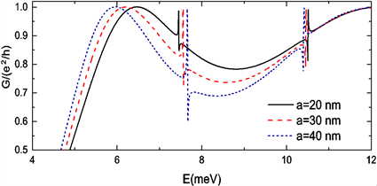
Figure 3. Conductance G as a function of E for different separation distance between two quantum wells for , , , , and
图3. 两量子阱间隔距离不同情况下电导G随入射能E的变化关系图。这里取 , , , , 和

Figure 4. Variation of Fano-type resonance line-shape in conductance G with for , , , , , and
图4. Fano型电导G随相位 的变化关系图。其中 , , , , , 和
这种情况下,对称共振峰将出现。
4. 总结
本文中,我们使用Floquet散射矩阵理论研究了Dirac电子在石墨烯时间周期双阱势中的共振隧穿。由于Dirac电子与振荡场之间相互作用,光助共振隧穿发生从而导致了尖锐的非对称Fano型共振峰的出现。非对称Fano型共振源自束缚态与连续态之间的量子干涉。数值计算的结果表明,Fano型共振谱在双阱势情况下将会劈裂为两个非对称共振峰,而且这两个峰的线型不相同。此外,两个振荡场的相对相位也可以改变非对称Fano型共振峰的线型。当相对相位从0增加到 时,共振峰的谷会从峰的一边移动到另外一边。在临界相对相位 处,非对称共振峰变为对称的峰。另外,振荡场的频率、振幅以及静势阱的结构都可以用来调制共振峰。这些特性可以用来实现对石墨烯中Dirac电子输运性质的调制。
基金项目
中国国家自然科学基金(11274102),教育部新世纪优秀人才支持计划(NCET-11-0960),教育部博士点基金(博导类) (20134208110001)。
文章引用
彭坦,周斌. 时间周期双阱势中光子辅助Dirac电子的Fano共振隧穿
Fano Resonance in Photon-Assisted Dirac Electron Transmission through a Time-Periodic Double-Well Potential[J]. 凝聚态物理学进展, 2017, 06(04): 86-95. http://dx.doi.org/10.12677/CMP.2017.64012
参考文献 (References)
- 1. Novoselov, K.S., Geim, A.K., Morozov, S.V., et al. (2005) Two-Dimensional Gas of Massless Dirac Fermions in Graphene. Nature, 438, 197-200. https://doi.org/10.1038/nature04233
- 2. Neto, A.H.C., Guinea, F., Peres, N.M.R., et al. (2009) The Electronic Properties of Graphene. Reviews of modern physics, 81, 109. https://doi.org/10.1103/RevModPhys.81.109
- 3. Rozhkov, A.V., Giavaras, G., Bliokh, Y.P., et al. (2011) Electronic Properties of Mesoscopic Graphene Structures: Charge Confinement and Control of Spin and Charge Transport. Physics Reports, 503, 77-114. https://doi.org/10.1016/j.physrep.2011.02.002
- 4. Semenoff, G.W. (1984) Condensed-Matter Simulation of a Three-Dimensional Anomaly. Physical Review Letters, 53, 2449. https://doi.org/10.1103/PhysRevLett.53.2449
- 5. Luk’yanchuk, I.A. and Kopelevich, Y. (2004) Phase Analysis of Quantum Oscilla-tions in Graphite. Physical Review Letters, 93, Article ID: 166402. https://doi.org/10.1103/PhysRevLett.93.166402
- 6. Zawadzki, W. and Rusin, T.M. (2011) Zitterbewegung (Trembling Motion) of Electrons in Semiconductors: A Review. Journal of Physics: Condensed Matter, 23, Article ID: 143201. https://doi.org/10.1088/0953-8984/23/14/143201
- 7. Cserti, J. and Dávid, G. (2006) Unified Description of Zitterbewegung for Spintronic, Graphene, and Superconducting systems. Physical Review B, 74, Article ID: 172305. https://doi.org/10.1103/PhysRevB.74.172305
- 8. Allain, P.E. and Fuchs, J.N. (2011) Klein Tunneling in Graphene: Optics with Massless Electrons. The European Physical Journal B, 83, 301. https://doi.org/10.1140/epjb/e2011-20351-3
- 9. De Leo, S. and Rotelli, P.P. (2006) Barrier Paradox in the Klein Zone. Physical Review A, 73, Article ID: 042107. https://doi.org/10.1103/PhysRevA.73.042107
- 10. De Leo, S. and Rotelli, P.P. (2007) Dirac Equation Studies in the Tunneling Energy Zone. The European Physical Journal C-Particles and Fields, 51, 241-247. https://doi.org/10.1140/epjc/s10052-007-0297-4
- 11. Sarma, S.D., Adam, S., Hwang, E.H., et al. (2011) Electronic Transport in Two-Dimensional Graphene. Reviews of Modern Physics, 83, 407. https://doi.org/10.1103/RevModPhys.83.407
- 12. Klein, O. (1929) Die Reflexion von Elektronen an Einem Potentialsprung Nach der Relativistischen Dynamik von Dirac. Zeitschriftfür Physik A Hadrons and Nuclei, 53, 157-165. https://doi.org/10.1007/BF01339716
- 13. Katsnelson, M.I., Novoselov, K.S. and Geim, A.K. (2006) Chiral Tunnelling and the Klein Paradox in Graphene. Nature Physics, 2, 620. https://doi.org/10.1038/nphys384
- 14. Barbiër, M., Papp, G., Peeters, F.M. (2012) Snake States and Klein Tunneling in a Gra-phene Hall Bar with a Pn-Junction. Applied Physics Letters, 100, Article ID: 163121. https://doi.org/10.1063/1.4704667
- 15. Pereira Jr, J.M., Mlinar, V., Peeters, F.M., et al. (2006) Confined States and Direc-tion-Dependent Transmission in Graphene Quantum Wells. Physical Review B, 74, Article ID: 045424. https://doi.org/10.1103/PhysRevB.74.045424
- 16. Bai, C. and Zhang, X. (2007) Klein Paradox and Resonant Tunneling in a Graphene Superlattice. Physical Review B, 76, Article ID: 075430. https://doi.org/10.1103/PhysRevB.76.075430
- 17. Park, C.H., Yang, L., Son, Y.W., et al. (2008) Anisotropic Behaviours of Massless Dirac Fermions in Graphene under Periodic Potentials. Nature Physics, 4.
- 18. Barbier, M., Vasilopoulos, P. and Peeters, F.M. (2010) Extra Dirac Points in the Energy Spectrum for Superlattices on Single-Layer Graphene. Physical Review B, 81, Article ID: 075438. https://doi.org/10.1103/PhysRevB.81.075438
- 19. Tan, L.Z., Park, C.H. and Louie, S.G. (2010) Graphene Dirac Fermions in One-Dimensional Inhomogeneous Field Profiles: Transforming Mag-netic to Electric Field. Physical Review B, 81, Article ID: 195426. https://doi.org/10.1103/PhysRevB.81.195426
- 20. Bliokh, Y.P., Freilikher, V., Savel’ev, S., et al. (2009) Transport and Localiza-tion in Periodic and Disordered Graphene Superlattices. Physical Review B, 79, Article ID: 075123. https://doi.org/10.1103/PhysRevB.79.075123
- 21. Cheianov, V.V., Fal’ko, V. and Altshuler, B.L. (2007) The Focusing of Elec-tron Flow and a Veselago Lens in Grapheme p-n Junctions. Science, 315, 1252-1255. https://doi.org/10.1126/science.1138020
- 22. Chiu, H.Y., Perebeinos, V., Lin, Y.M., et al. (2010) Controllable p-n Junction Formation in Monolayer Graphene using Electrostatic Substrate Engineering. Nano Letters, 10, 4634-4639. https://doi.org/10.1021/nl102756r
- 23. Han, M.Y., Özyilmaz, B., Zhang, Y., et al. (2007) Energy Band-Gap Engineering of Graphemenanoribbons. Physical Review Letters, 98, Article ID: 206805. https://doi.org/10.1103/PhysRevLett.98.206805
- 24. Huard, B., Sulpizio, J.A., Stander, N., et al. (2007) Transport Measurements across a Tunable Potential Barrier in Graphene. Physical Review Letters, 98, Article ID: 236803. https://doi.org/10.1103/PhysRevLett.98.236803
- 25. Ghosh, T.K., De Martino, A., Häusler, W., et al. (2008) Conductance Quantiza-tion and Snake States in Graphene Magnetic Waveguides. Physical Review B, 77, Article ID: 081404. https://doi.org/10.1103/PhysRevB.77.081404
- 26. Fano, U. (1961) Effects of Configuration Interaction on Intensities and Phase Shifts. Physical Review, 124, 1866. https://doi.org/10.1103/PhysRev.124.1866
- 27. Miroshnichenko, A.E., Flach, S. and Kivshar, Y.S. (2010) Fano Resonances in Nanoscale Structures. Reviews of Modern Physics, 82, 2257. https://doi.org/10.1103/RevModPhys.82.2257
- 28. Dayem, A.H. and Martin, R.J. (1962) Quantum Interaction of Microwave Radiation with Tunneling between Superconductors. Physical Review Let-ters, 8, 246. https://doi.org/10.1103/PhysRevLett.8.246
- 29. Tien, P.K. and Gordon, J.P. (1963) Multiphoton Process Observed in the Interaction of Microwave Fields with the Tunneling between Superconductor Films. Physical Review, 129, 647. https://doi.org/10.1103/PhysRev.129.647
- 30. Büttiker, M. and Landauer, R. (1982) Traversal Time for Tunneling. Physical Re-view Letters, 49, 1739. https://doi.org/10.1103/PhysRevLett.49.1739
- 31. Wagner, M. (1996) Strongly Driven Quantum Wells: An Analytical Solution to the Time-Dependent Schrödinger Equation. Physical Review Letters, 76, 4010. https://doi.org/10.1103/PhysRevLett.76.4010
- 32. Wagner, M. and Zwerger, W. (1997) Characteristic Scaling Parameters for Tunnel-ing in Strong Time-Dependent Electric Fields. Physical Review B, 55, R10217. https://doi.org/10.1103/PhysRevB.55.R10217
- 33. Burmeister, G. and Maschke, K. (1998) Scattering by Time-Periodic Potentials in One Dimension and Its Influence on Electronic Transport. Physical Review B, 57, 13050. https://doi.org/10.1103/PhysRevB.57.13050
- 34. Burmeister, G. and Maschke, K. (1999) Bound States Revealed by Time-Periodic Perturbing Scattering Potentials. Physical Review B, 59, 4612. https://doi.org/10.1103/PhysRevB.59.4612
- 35. Li, W. and Reichl, L.E. (1999) Floquet Scattering through a Time-Periodic Potential. Physical Review B, 60, Article ID: 15732. https://doi.org/10.1103/PhysRevB.60.15732
- 36. Moskalets, M. and Büttiker, M. (2002) Floquet scattering Theory of Quantum Pumps. Physical Review B, 66, Article ID: 205320. https://doi.org/10.1103/PhysRevB.66.205320
- 37. Shelykh, I.A. and Galkin, N.G. (2004) Fano and Breit-Wigner Resonances in Carrier Transport through Datta and Das Spin Modulators. Physical Review B, 70, Article ID: 205328. https://doi.org/10.1103/PhysRevB.70.205328
- 38. Ho, C.L. and Lee, C.C. (2005) Stabilizing Quantum Met-astable States in a Time-Periodic Potential. Physical Review A, 71, Article ID: 012102. https://doi.org/10.1103/PhysRevA.71.012102
- 39. Zhang, C.X., Nie, Y.H. and Liang, J.Q. (2006) Photon-Assisted Electron Trans-mission Resonance through a Quantum Well with Spin-Orbit Coupling. Physical Review B, 73, Article ID: 085307. https://doi.org/10.1103/PhysRevB.73.085307
- 40. Ye, C.Z., Zhang, C.X., Nie, Y.H., et al. (2007) Field-Assisted Resonance Tunneling through a Symmetric Double-Barrier Structure with Spin-Orbit Coupling. Physical Review B, 76, Article ID: 035345. https://doi.org/10.1103/PhysRevB.76.035345
- 41. Zhang, C.X., Nie, Y.H. and Liang, J.Q. (2008) Field-Assisted Electron Transport through a Symmetric Double-Well Structure with Spin Orbit Coupling and the Fano-Resonance Induced Spin Filtering. Chi-nese Physics B, 17, 2670-2677. https://doi.org/10.1088/1674-1056/17/7/052
- 42. Hu, L.Y. and Zhou, B. (2011) Spin-Dependent Breit-Wigner and Fano Reso-nances in Photon-Assisted Electron Transport through a Semiconductor Heterostructure. Chinese Physics B, 20, Article ID: 067201. https://doi.org/10.1088/1674-1056/20/6/067201
- 43. Reinhardt, J. and Greiner, W. (1977) Quantum Electrodynamics of Strong Fields. Reports on Progress in Physics, 40, 219. https://doi.org/10.1088/0034-4885/40/3/001
- 44. Petrillo, V. and Janner, D. (2003) Relativistic Analysis of a Wave Packet Interacting with a Quantum-Mechanical Barrier. Physical Review A, 67, Article ID: 012110. https://doi.org/10.1103/PhysRevA.67.012110
- 45. Trauzettel, B., Blanter, Y.M. and Morpurgo, A.F. (2007) Pho-ton-Assisted Electron Transport in Graphene: Scattering Theory Analysis. Physical Review B, 75, Article ID: 035305. https://doi.org/10.1103/PhysRevB.75.035305
- 46. Zeb, M.A., Sabeeh, K. and Tahir, M. (2008) Chiral Tunneling through a Time-Periodic Potential in Monolayer Graphene. Physical Review B, 78, Article ID: 165420. https://doi.org/10.1103/PhysRevB.78.165420
- 47. Cao, Z., Cheng, Y. and Li, G.Q. (2011) Massive Dirac Electron Tunneling through a Time-Periodic Potential in Single Layer Graphene. Physics Letters A, 375, 4065-4069. https://doi.org/10.1016/j.physleta.2011.08.074
- 48. Wu, Z., Li, J. and Chan, K.S. (2012) Charge Pumping in Monolayer Graphene Driven by a Series of Time-Periodic Potentials. Physics Letters A, 376, 1159-1165. https://doi.org/10.1016/j.physleta.2012.01.043
- 49. Savel’ev, S.E., Häusler, W. and Hänggi, P. (2012) Current Resonances in Gra-phene with Time-Dependent Potential Barriers. Physical Review Letters, 109, Article ID: 226602. https://doi.org/10.1103/PhysRevLett.109.226602
- 50. Lu, W.T., Wang, S.J., Li, W., et al. (2012) Fano-Type Resonance through a Time-Periodic Potential in Graphene. Journal of Applied Physics, 111, Article ID: 103717. https://doi.org/10.1063/1.4721653
- 51. Sinha, C. and Biswas, R. (2012) Transmission of Electron through Monolayer Graphene Laser Barrier. Applied Physics Letters, 100, Article ID: 183107. https://doi.org/10.1063/1.4710525
- 52. Myoung, N., Seo, K. and Ihm, G. (2013) Demonstration of Magnetic Confinement in Graphene with Fano-Type Resonances. Journal of the Korean Physical Society, 62, 275-283. https://doi.org/10.3938/jkps.62.275
- 53. Szabó, L.Z., Benedict, M.G., Czirják, A., et al. (2013) Relativistic Electron Transport through an Oscillating Barrier: Wave-Packet Generation and Fano-Type Resonances. Physical Review B, 88, Article ID: 075438. https://doi.org/10.1103/PhysRevB.88.075438
- 54. Biswas, R. and Sinha, C. (2013) Photon Induced Tunneling of Electron through a Graphene Electrostatic Barrier. Journal of Applied Physics, 114, Article ID: 183706. https://doi.org/10.1063/1.4829446
- 55. Biswas, R. and Sinha, C. (2014) Spin Orbit Splitting of the Photon Induced Fano Reso-nance in an Oscillating Graphene Electrostatic Barrier. Journal of Applied Physics, 115, Article ID: 133705. https://doi.org/10.1063/1.4869846
- 56. Zhang, C., Liu, J. and Fu, L. (2015) Anomalous Fano Resonance of Massive Dirac Parti-cle through a Time-Dependent Barrier. Europhysics Letters, 110, Article ID: 61001. https://doi.org/10.1209/0295-5075/110/61001
- 57. Biswas, R., Maity, S. and Sinha, C. (2016) Beating Oscillation and Fano Resonance in the Laser Assisted Electron Transmission through Graphene δ-Function Magnetic Barriers. Physica E: Low-Dimensional Systems and Nanostructures, 84, 235-243. https://doi.org/10.1016/j.physe.2016.06.010
- 58. Biswas, R., Maiti, S., Mukhopadh-yay, S, et al. (2017) Electron Transmission through a Periodically Driven Graphene Magnetic Barrier. Physics Letters A, 381, 1582-1591. https://doi.org/10.1016/j.physleta.2017.02.045
- 59. Shirley, J.H. (1965) Solution of the Schrödinger Equation with a Hamiltonian Periodic in Time. Physical Review, 138, B979. https://doi.org/10.1103/PhysRev.138.B979
- 60. Holthaus, M. and Hone, D. (1993) Quantum Wells and Superlattices in Strong Time-Dependent Fields. Physical Review B, 47, 6499. https://doi.org/10.1103/PhysRevB.47.6499
- 61. Fromherz, T. (1997) Floquet States and Intersubband Absorption in Strongly Driven Double Quantum Wells. Physical Review B, 56, 4772. https://doi.org/10.1103/PhysRevB.56.4772
- 62. Bagwell, P.F. and Lake, R.K. (1992) Resonances in Transmission through an Oscillating Barrier. Physical Review B, 46, Article ID: 15329. https://doi.org/10.1103/PhysRevB.46.15329
- 63. Landauer, R. (1989) Conductance Determined by Transmission: Probes and Quantised Constriction Resistance. Journal of Physics: Condensed Matter, 1, 8099. https://doi.org/10.1088/0953-8984/1/43/011
- 64. Büttiker, M. (1986) Four-Terminal Phase-Coherent Conductance. Physical Re-view Letters, 57, 1761. https://doi.org/10.1103/PhysRevLett.57.1761
- 65. Christen, T. and Büttiker, M. (1996) Low Frequency Admittance of a Quantum Point Contact. Physical Review Letters, 77, 143. https://doi.org/10.1103/PhysRevLett.77.143
- 66. Bulgakov, E.N. and Sadreev, A.F. (1996) Current-Voltage Characteristics of the Resonant Tunnelling Double-Barrier Structure under Time-Periodical Perturbation. Journal of Physics: Condensed Matter, 8, 8869. https://doi.org/10.1088/0953-8984/8/45/020
- 67. Göres, J., Goldhaber-Gordon, D., Heemeyer, S., et al. (2000) Fano Resonances in Electronic Transport through a Single-Electron Transistor. Physical Review B, 62, 2188. https://doi.org/10.1103/PhysRevB.62.2188
- 68. Kobayashi, K., Aikawa, H., Katsumoto, S., et al. (2002) Tuning of the Fano Effect through a Quantum Dot in an Aharonov-Bohm Interferometer. Physical Review Letters, 88, Article ID: 256806. https://doi.org/10.1103/PhysRevLett.88.256806
- 69. Kobayashi, K., Aikawa, H., Katsumoto, S., et al. (2003) Mesoscopic Fano Effect in a Quantum Dot Embedded in an Aharonov-Bohmring. Physical Review B, 68, Article ID: 235304. https://doi.org/10.1103/PhysRevB.68.235304
- 70. Racec, E.R. and Wulf, U. (2001) Resonant Quantum Transport in Semiconductor Nanostructures. Physical Review B, 64, Article ID: 115318. https://doi.org/10.1103/PhysRevB.64.115318