Open Journal of Circuits and Systems
Vol.06 No.04(2017), Article ID:23093,7
pages
10.12677/OJCS.2017.64014
DC Internal Inductance Analysis Formula
Baojun Chen, Yanjie Ju
School of Electronics and Information Engineering, Dalian Jiaotong University, Dalian Liaoning

Received: Nov. 28th, 2017; accepted: Dec. 14th, 2017; published: Dec. 21st, 2017

ABSTRACT
In the super-large-scale integration, the influence of interconnecting wire inductance effect on the circuit performance is increasingly obvious as the clock frequency increases, the signal rise time decreases and the copper technology is adopted. Both the moment method and high-order basis function method are the numerical methods with the advantage of accurate computing result and disadvantage of low computing efficiency. Therefore, the paper proposes a analysis formula of the dc internal and the formula can improve the computing efficiency.
Keywords:Interconnect, Inductance, IC
直流内部电感解析式
陈宝君,鞠艳杰
大连交通大学电气信息学院,辽宁 大连
收稿日期:2017年11月28日;录用日期:2017年12月14日;发布日期:2017年12月21日

摘 要
在超大规模集成电路中,随着时钟频率的增加、信号上升时间的缩短以及铜工艺的采用,互连线电感效应对电路性能的影响越来越突出。矩量法和高阶基函数法均为数值方法,其优点是计算结果准确,但缺点是计算效率低,为此本文给出了直流内部电感计算的解析式,该公式可快速准确计算直流内部电感值,提高参数提取效率。
关键词 :互连线,电感,集成电路

Copyright © 2017 by authors and Hans Publishers Inc.
This work is licensed under the Creative Commons Attribution International License (CC BY).
http://creativecommons.org/licenses/by/4.0/


1. 引言
由于趋肤效应的存在,导致互连线上有寄生参数产生,这些寄生参数是随频率变化的。而在数字信号分析中采用时域分析较为方便,因此需要用与频率无关的电路模型来表示趋肤效应。图1为使用与频率无关的电阻电感组成的电路模型 [1] [2] 。
其中, 为外部电感, 为与直流内部电感 有关的电感值,且图1(b)中 , , 。在以上等效电路模型中均用到了内部电感和外部电感,因此内部电感和外部电感的解析式是这些电路模型的重要参数。
导线的内部和外部都有场的存在,因此电感可以分为内部电感和外部电感。内部电感和外部电感的定义为 [3] [4] :
, (1)
其中, 分别为导线内部和外部的总磁通量, 为导体中的电流。
导线的电感为内部电感和外部电感之和,即:
(2)
在直流情况下,电流均匀分布在导线中,导线的内部外部均有磁场存在,此时的电感为直流电感,可表示为:
(3)
其中, 为直流电感。
当频率非常高时,由于趋肤效应的影响,电流全部聚集的导线的表面,导线内部没有场的存在,可以近似的认为此时的内部电感为0。外部电感是与高频率电感的极限值相对应的,此时可以认为是极限情况。即:
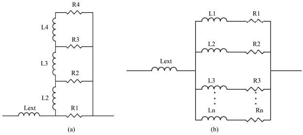
Figure 1. Equivalent circuit for skin-effect
图1. 描述趋肤效应的电路模型
, (4)
为高频时电感值。该式表明外部电感等于高频率时的电感值。
外部电感的大小取决于导线本身的尺寸,不随频率变化,则内部电感是高频和低频电感值的差值 [5] [6] [7] :
(5)
使用矩量法计算内部电感值需要大量的计算时间,因此需要提出简单的解析公式,用以应用到电路模型中。目前内部电感计算解析式有:
(6)
(7)
公式(6)为单位长度的圆形截面导线内部电感计算公式 [8] [9] [10] ,而目前集成电路中互连线均为矩形截面。公式(7)为矩形导线的内部电感计算公式 [11] ,但该公式在计算时误差较大。
2. 直流内部电感的数值计算结果
为了得到矩形截面导线的内部电感解析式,我们需要通过数值方法,使用公式(5)得到内部电感值。
使用矩量法,可以得到矩形截面导线的单位长度电感值。直流电感是频率较低时的电感值,将频率取值为1 Hz即可得到直流电感值。图2为导线厚度为0.005 μm到1000 μm时,正方形截面导线的直流电感值。由该图可知直流电感值取决于导线的尺寸,并且随着导线尺寸的增加,直流电感值逐渐减小。
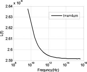
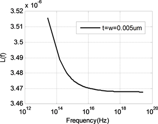
由前面分析可知,随着频率的升高,内部电感逐渐减小,当内部电感减小到零时,导线的电感值等于外部电感。内部电感为零时,频率非常高,使得电流全部聚集在导线表面,对于多数导体来说这是一种极限情况。因此计算外部电感首先要选择频率,图3为使用矩量法计算得到的不同尺寸导线电感值随频率变化曲线,如图所示,随着频率的升高,电感值减小而且逐渐趋于恒定值。当电感达到恒定值,不再随频率变化时,可以认为这时的内部电感为零,此时导线电感即为外部电感。根据大量的计算结果,得到外部电感的频率计算公式为:
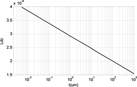
Figure 2. The direct inductance of different line
图2. 不同尺寸互连线的直流电感值
 (a)
(a)
 (b)
(b)
 (c)
(c)
 (d)
(d)
Figure 3. The inductance of different line
图3. 不同尺寸导线的电感值
(8)
其中, 为转折角频率。
选取好最高频率后,可以使用矩量法得到外部电感值,然后利用公式(5)来计算不同尺寸互连线的内部电感。不同尺寸导线的内部电感值如图4所示。当导线的宽长比为1,即正方形截面导线的内部电感与导线的尺寸是无关的,不论导线尺寸是多少内部电感值都是5.55e−8H。而对于任意的矩形截面导线,内部电感值主要是宽长比的函数,只与宽长比有关。
图5为不同导线内部电感的相对误差,相对误差计算公式为:
(9)
其中, 。
从图中可以看出,当宽长比较小时,不同尺寸导线的内部电感会有所差异,但是这个差异最大不超过0.08%。因此我们可以认为不同尺寸导线的内部电感在宽长比相同时内部电感是相同的,即内部电感计算公式仅以宽长比为变量。
3. 直流内部电感计算公式
从内部电感随宽长比变化的图形可以看出,整个变化曲线可以分成两个部分,当宽长比较小时,内
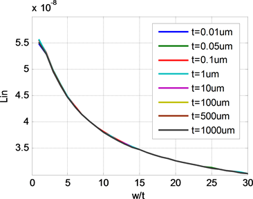
Figure 4. The internal inductance of different line
图4. 不同尺寸互连线内部电感值
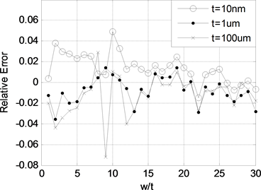
Figure 5. The relative error of internal inductance
图5. 内部电感的相对误差
部电感减小速度较快,随着宽长比的增加,曲线变化趋于平缓,为此我们使用两个函数的组合来拟合内部电感值。
为了描述图形的右侧部分,本文使用有理函数进行拟合:
(10)
其中, 为宽长比,系数 可以通过最小二乘法得到,其值为: ,
, , 。
图6为公式(10)计算结果与矩量法结果的误差,从图中可以看出,宽长比较大时,二者拟合较好,而宽长比小时,公式(10)计算误差较大。因此,对左侧曲线我们需要另外寻找拟合函数。这部分我们使用拉格朗日法对图6所示的误差进行拟合。拉格朗日插值法是根据n + 1个点 的函数值 推出n次多项式 ,然后由多项式 求出任意的点x对应的函数值 的算法。具体计算步骤为:
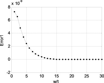
Figure 6. The error between Formula (10) and MOM
图6. 公式(10)与矩量法结果的误差
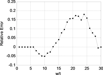
Figure 7. The error of the Formula (13)
图7. 公式(13)的误差
对于某个多项式函数,已知有给定的k + 1个取值点:
其中, 对应着自变量的位置,而 对应着函数在这个位置的取值。
假设任意两个不同的 都互不相同,那么应用拉格朗日插值公式所得到的拉格朗日插值多项式为:
(11)
其中,每个 为拉格朗日基本多项式,其表达式为:
(12)
根据拉格朗日方法我们使用七个采样点,得到内部电感左侧图形的拟合公式为:
(13)
其中, ,式中的系数为 , , , , , , 。
图7为拟合公式的误差,可以看出该公式的最大误差不超过0.2%,满足计算精度要求。
4. 结论
本文首先根据矩量法结果,使用最小二乘结合拉格朗日方法得到了内部电感解析式,该公式可应用在模拟趋肤效应的电路模型中,为在时域内进行参数提取提供方便。
文章引用
陈宝君,鞠艳杰. 直流内部电感解析式
DC Internal Inductance Analysis Formula[J]. 电路与系统, 2017, 06(04): 111-117. http://dx.doi.org/10.12677/OJCS.2017.64014
参考文献 (References)
- 1. Nei, S. and Ismail, Y.I. (2003) Modeling Skin Effect with Reduced Decoupled R-L Circuits Circuits and Systems. International Symposium on Circuits & Systems, 4, 588-591.
- 2. Choudhury, J. and Seetharaman, G.S. (2003) Accurate Modeling of Thin-Film Inductance for Nano-Chip. Nanotechnology IEEE-NANO Third IEEE Conference on Nanotechnology, 1, 351-355. https://doi.org/10.1109/NANO.2003.1231790
- 3. Maheshwaril, V. and Lacanial, S. (2011) An Explicit Crosstalk Aware Delay Modeling for on-Chip VLSI RLC Interconnect with Skin Effect. Journal of Electron Devices, 10, 499-505.
- 4. Mei, S. and Amin, C. (2003) Efficient Model Order Reduction Including Skin Effect. Design Automation Conference, 27, 232-237. https://doi.org/10.1145/775832.775892
- 5. Huerta, C.J. (2009) A Modified Model for the Self Inductance of Metal Lines on Si. IEEE Mtt-s International Microwave Workshop Series on Signal Integrity & High-speed Interconnects, 111-114. https://doi.org/10.1109/IMWS.2009.4814920
- 6. Modal, M. and Massoud, Y. (2005) Analytical Modeling of Loop Self Inductance Bound for Inductance-Aware Physical Synthesis. Circuits and Systems, 2, 1721-1724.
- 7. Chung, K. (2000) Interconnect Analysis and Synthesis. Wiley- Interscience Press, New York.
- 8. Grover, F. (1962) Inductance Calculations: Working Formulas and Tables. Dover Press, New York.
- 9. Hoer, C. and Loce, C. (1965) Exact Inductance Equations for Rectangular Conductors with Applications to More Complicated Geometries. Journal of Research of the National Bureau of Standards, 69, 127-137. https://doi.org/10.6028/jres.069C.016
- 10. Kim, H. Be Careful of Self and Mutual Inductance Formu-lae.
- 11. Hsiao, Y. (2009) A Physical De-embedding Method for Silicon-based Device Applications. Piers Online, 5, 301-305. https://doi.org/10.2529/PIERS080907133328