Journal of Advances in Physical Chemistry
Vol.
13
No.
01
(
2024
), Article ID:
77911
,
7
pages
10.12677/JAPC.2024.131001
外加电场对空位缺陷下硫硒化钼/石墨烯异质 结构的电子性质调控
张康新,王远帆,谢泉
贵州大学大数据与信息工程学院,新型光电子材料与技术研究所,贵州 贵阳
收稿日期:2023年11月10日;录用日期:2023年12月14日;发布日期:2023年12月25日

摘要
本文构建了四种由Janus MoSSe和Graphene垂直堆垛而成的含缺陷异质结构。基于密度泛函理论的第一性原理计算方法研究了外加电场对空位缺陷下Janus MoSSe/Grahene异质结构电子性质的影响。研究发现S空位缺陷下的SMoSe/Graphene异质结构在电场的作用下可以改变其掺杂类型,最高能够达到1.176 × 1013 cm−2的n-type掺杂密度。SeMoS/Graphene的S和Se空位缺陷结构在电场作用下能分别达到1.488 × 1013 cm−2和1.555 × 1013 cm−2的载流子掺杂密度,并且施加反向的电场能够完全抑制掺杂的产生。
关键词
第一性原理,异质结构,外加电场,电子性质

Regulation of the Electronic Properties of the MoSSe/Graphene Heterostructure under Vacancy Defects by the Applied Electric Field
Kangxin Zhang, Yuanfan Wang, Quan Xie
Institute of New Optoelectronic Materials and Technology, College of Big Data and Information Engineering, Guizhou University, Guiyang Guizhou
Received: Nov. 10th, 2023; accepted: Dec. 14th, 2023; published: Dec. 25th, 2023

ABSTRACT
In this paper, four defective heterostructures composed of Janus MoSSe and Graphene vertical stacking are constructed. The effect of the applied electric field on the electronic properties of the Janus MoSSe/Grahene heterostructure under vacancy defects is studied by the first-principles calculation method based on density functional theory. It is found that the SMoSe/Graphene heterostructure under the S vacancy defect can change its doping type under the action of electric field, and the maximum n-type doping density of 1.176 × 1013 cm−2 can be reached. The S and Se vacancy defect structures of SeMoS/Graphene can reach the carrier doping density of 1.488 × 1013 cm−2 and 1.555 × 1013 cm−2 respectively under the action of electric field, and the application of the opposite electric field can completely inhibit the generation of doping.
Keywords:First Principles, Heterostructure, The Applied Electric Field, Electronic Properties

Copyright © 2024 by author(s) and Hans Publishers Inc.
This work is licensed under the Creative Commons Attribution International License (CC BY 4.0).
http://creativecommons.org/licenses/by/4.0/


1. 引言
2004年,石墨烯成功在实验室中被剥离出来,二维材料以其优越的光子 [1] 、电子 [2] 、压电 [3] 等性质成为了研究人员的重点关注目标。许多种二维材料已经在实验中成功制备,例如黑鳞 [4] 、蓝磷 [5] 、过渡金属硫化物 [6] (transition metal dichalcogenides, TMDs)等。二维材料还可以通过互相垂直堆叠构组成异质结构。这些异质结构具备着其单层二维材料所没有的优点。近年来,二维Janus材料的兴起,在基于第一性原理计算的二维材料理论计算中掀起了研究的热潮。其中JanusTMDs及其异质结构在磁性材料 [7] ,光催化分解水 [8] [9] [10] [11] ,纳米电子器件 [12] [13] [14] ,气体传感器 [15] [16] ,太阳能电池 [17] 等领域中展现了潜在的应用前景。同时,在实验上,二维材料的制备也得到了很大的推进,在传统理论计算中只考虑本征结构去进行电子性质的分析不足以应对在制备二维材料时可能出现的一些实际情况。杂质以及各类缺陷会伴随材料的制备而产生,通过理论计算去模拟实际情况并考虑其带来的影响能够很好指导实验的制备时应该关注的重点问题。同时,实验上缺陷的识别一般是困难且间接的,通常需要不同技术的巧妙结合才得以实现。如今第一性原理计算已经被证明是能够指导实验的有力方法,并且具有足够的可靠性可以作为预测缺陷的工具 [18] 。在Janus二维过渡金属硫属化物及其异质结构的研究结果中,相关的空位缺陷工程调控的工作进展仍为空白。本文的工作将对此项有待深入讨论的内容进行研究,旨在能够为二维Janus MoSSe在光电子和纳米电子器件的发展中提供一定的理论指导。对二维材料施加垂直方向的电场是用来调控二维材料电学性能的一种常用方法。特别作用在异质结构中,垂直方向的电场能够有效的调节层间的电荷转移,实现调控层间的电荷转移等性质。在外界条件下,异质结构中的Graphene狄拉克锥的位置通常是可以进行调控的,Deng等人通过改变层间距离和在z方向施加外加电场来改变狄拉克锥的位置,成功调控Graphene的载流子掺杂密度 [19] 。Wang等人通过施加双轴应变在缺陷异质结构上有效调控了石墨烯的载流子浓度 [20] 。
2. 计算方法
在MaterialStudio软件以及Vesta可视化软件中进行异质结构模型的构建,导出模型数据后基于VASP软件包进行第一性原理计算,整个计算采用基于密度泛函理论的投影缀加平面波(PAW)的赝势方法 [21] ,电子的交换相关泛函采用广义梯度近(GGA)似下的Perdue-Burke-Ernzerhof (PBE)泛函来表示 [22] 。在进行收敛性测试后,将平面波截断能设置为500 eV。所有结构被完全弛豫后,定义了相邻电子步能量差和离子步中原子之间作用力的收敛标准分别被定义为10−7 eV和10−3 eV/Å。为了消除周期性势场对二维材料的影响,构建模型时在垂直方向加入了20 Å的真空层。结构优化中布里渊区采样使用了9 × 9 × 1 Monkhorst-Pack的k点网络,电子自洽时采用12 × 12 × 1的k点网络。VASP中外加电场的方法是基于电子自洽的电荷密度文件CHGCAR文件和波函数文件WAVECAR,对添加电场参数的结构进行后续的计算,通过在INCAR中设置LDIPOL,并添加IDIPOL = 3参数,考虑计算时在z方向的偶极矩,将电场方向也设定为z方向。电场强度则是通过EFIELD参数进行设定大小,并且设置DIPOL去修正偶极子在二维材料体系中的位置,使电子步更加容易收敛。
3. 结果与讨论
3.1. 结构模型与稳定性研究
将MoSSe和Graphene两种单层材料堆叠成异质结构,由于MoSSe材料的不对称性,可以堆叠出两种结构,分别为SMoSe/Graphene和SeMoS/Graphene异质结构。为了确保异质结构的晶格失配率小于3%,我们需要对两种晶格常数不同的材料进行扩胞。MoSSe的晶格常数为3.25 Å,进行2 × 2的扩胞,扩胞后的晶格常数为6.53 Å。Graphene的晶格常数为2.46 Å,进行√7 × √7的扩胞,扩胞后的晶格常数为6.50 Å。计算得出的晶格失配率仅为0.46%。在该两种异质结构上引入S缺陷和Se缺陷,分别具有S和Se空位缺陷的MoSSe与Graphene组合成不同的异质结堆叠模式,一共可以组成四种不同的含空位缺陷异质结构模型。如图1所示。S缺陷和Se缺陷下,SMoSe/Graphene堆叠模式的含空位缺陷异质结构分别表示为SMoSe_VS/Graphene和SMoSe_VSe/Graphene。而SeMoS/Graphene堆叠模式的含空位缺陷异质结构表示为SeMoS_VS/Graphene和SeMoS_VSe/Graphene。考虑异质结构层间范德华作用后完成结构优化,得到稳定结构后的缺陷周围的键长键角,异质结构层间距以及根据结合能计算的能量列于表1中。计算所得的结合能为负值,说明构建的四种异质结构整体能量在降低达到稳定状态。

Figure 1. Janus MoSSe/Graphene heterostructure model with vacancy defects
图1. 含空位缺陷的Janus MoSSe/Graphene异质结构模型
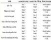
Table 1. Contains the Mo-S bond length and Mo-Se bond length, layer spacing and binding energy in the vicinity of the vacancy defect heterostructure
表1. 含空位缺陷异质结构中,空位缺陷附近的Mo-S键长和Mo-Se键长,异质结构层间距和结合能
3.2. 外加电场对异质结电荷载流子调控
过大的外加电场可能会击穿二维材料,对计算模型带来很大的干扰。选用在合理范围内的−0.6 V/Å到0.6 V/Å的电场强度对含缺陷的异质结构进行调控,以每0.2 V/Å为一个节点,观察在各个电场区间内不同异质结构的能带结构的变化。在SMoSe/Graphene堆叠模式的异质结构中,定义层间电子移动方向为电场的正方向,即Graphene指向MoSSe。图2中分别计算了SMoSe/Graphene堆叠模式下S和Se空位缺陷在各个电场区间的能带图。在SMoSe_VS/Graphene和SMoSe_VSe/Graphene的初始状态狄拉克锥处于费米能级位置 [20] ,从图中可以看到随着正向电场的加大狄拉克锥的位置都发生了向上的位移。在S缺陷下,负向电场也使得狄拉克锥位置随之下降到费米能级之下,形成了Graphene的n-type电子掺杂。而Se缺陷在−0.2 V/Å和−0.4 V/Å Graphene部分的能带没有发生变化,但是扩大 肖特基势垒,在−0.6 V/Å电场下也产生了n-type掺杂。可见外加电场能够有效改变层间电子的移动,从而使掺杂类型发生变化,此外S缺陷异质结构比Se缺陷异质结构对电场强度变化更加敏感。

Figure 2. (a) SMoSe_Vs/Graphene and (b) SMoSe_Vse/Graphene heterogeneous band plots under applied electric fields (E = −0.6, −0.4, −0.2, 0.2, 0.4, 0.6 V/Å)
图2. (a) SMoSe_Vs/Graphene和(b) SMoSe_Vse/Graphene异质结构在外加电场(E = −0.6, −0.4, −0.2, 0.2, 0.4, 0.6 V/Å)下的能带图
图3中分别计算了SeMoS/Graphene堆叠模式下S和Se空位缺陷在各个电场区间的能带图。在SeMoS/Graphene堆叠模式中,由于异质结构建模时与SMoSe/Graphene堆叠模式在z方向上的位置不同,Graphene与MoSSe的位置发生了交换,故在此堆叠模式下,电场的正方向被定义为MoSSe指向Graphene,与层间电子移动方向相反。随着负向电场的加大,狄拉克锥在此基础上继续向上位移,加大了p-type掺杂的密度。而正向电场则与初始状态的掺杂形成的抵消,狄拉克锥向下位移,在SeMoS_VS/Graphene中,0.4 V/Å的电场强度使得狄拉克锥回到本征时的费米能级位置,而0.6 V/Å让Graphene发生了n-type掺杂。在SeMoS_VSe/Graphene中,0.6 V/Å的电场强度才能使得狄拉克锥处于费米能级。

Figure 3. Bands of (a) SeMoS_Vs/Graphene and (b) SeMoS_Vse/Graphene heterostructures under applied electric fields (E = −0.6, −0.4, −0.2, 0.2, 0.4, 0.6 V/Å)
图3. (a) SeMoS_Vs/Graphene和(b) SeMoS_Vse/Graphene异质结构在外加电场(E = −0.6, −0.4, −0.2, 0.2, 0.4, 0.6 V/Å)下的能带
为了将电场调控Graphene电荷载流子掺杂的具体数值表现出来,将能带图的表现转换为载流子掺杂密度,如图4所示。在这项工作中,统一了不同堆叠模式的外加电场与层间电子转移的方向,规定电场负方向与层间电子转移方向一致,这样能够帮助我们更好分析外加电场对异质结构的影响。计算得出,电场方向确实能够促进或者阻碍层间电子的转移,促使Graphene的掺杂密度发生改变,甚至还能改变Graphene电荷载流子掺杂类型发生改变。对于SMoSe_VSe/Graphene中,将Graphene掺杂类型改变需经历一定电场强度的阈值,说明在这种堆叠模式下,S缺陷会比Se缺陷对Graphene的p-type掺杂更加敏感。SMoSe_VS/Graphene异质结构是最适合外加电场调控Graphene掺杂密度,能够同时具备n-type及p-type的掺杂类型,并且在n-type掺杂中电子掺杂浓度达到1.176 × 1013 cm−2。在无外加电场情况下就具备载流子掺杂的SeMoS_Vs/Graphene和SeMoS_VSe/Graphene异质结构中,电场能够加强掺杂的载流子密度,在0.6 V/Å下,能够将密度提升到1.488 × 1013 cm−2和1.555 × 1013 cm−2,并且反向的外加电场能够有效抑制电荷载流子掺杂的发生。

Figure 4. Charge carrier doping density of a heterostructure with vacancy defects in an applied electric field (E = −0.6, −0.4, −0.2, 0.2, 0.4, 0.6 V/Å)
图4. 含空位缺陷的异质结构在外加电场(E = −0.6, −0.4, −0.2, 0.2, 0.4, 0.6 V/Å)下Graphene的电荷载流子掺杂密度
4. 结论
通过对SMoSe_VS/Graphene、SMoSe_VSe/Graphene、SeMoS_VS/Graphene和SeMoS_VSe/Graphene四种含缺陷的异质结构施加z方向的电场进行调控,电场强度控制在0.6 V/Å内。外加的电场能够很好地调节异质结构的层间电子排布,实现电荷载流子掺杂密度以及类型的调控。SMoSe_VS/Graphene能够很好地适应电场调控掺杂密度,在正负电场的作用下能够轻易改变掺杂类型,并且最高能够实现1.176 × 1013 cm−2的n-type掺杂密度。SeMoS/Graphene的S和Se空位缺陷结构在电场作用下能分别达到1.488 × 1013 cm−2和1.555 × 1013 cm−2的载流子掺杂密度,并且施加反向的电场能够完全抑制掺杂的产生。本文从施加外加电场方面实现对含有S或Se原子空位缺陷的SMoSe/Graphene和SeMoS/Graphene异质结构进行电荷载流子密度调控。该项工作有益于调控载流子密度的研究,对高速载流子纳米器件和光电子器件的研究有着一定的参考价值。
文章引用
张康新,王远帆,谢 泉. 外加电场对空位缺陷下硫硒化钼/石墨烯异质结构的电子性质调控
Regulation of the Electronic Properties of the MoSSe/Graphene Heterostructure under Vacancy Defects by the Applied Electric Field[J]. 物理化学进展, 2024, 13(01): 1-7. https://doi.org/10.12677/JAPC.2024.131001
参考文献
- 1. Sangwan, V.K. and Hersam, M.C. (2018) Electronic Transport in Two-Dimensional Materials. Annual Review of Physical Chemistry, 69, 299-325. https://doi.org/10.1146/annurev-physchem-050317-021353
- 2. Taft, E.A. and Philipp, H.R. (1965) Optical Properties of Graphite. Physical Review, 138, A197. https://doi.org/10.1103/PhysRev.138.A197
- 3. Duerloo, K.N., Ong, M.T. and Reed, E.J. (2012) Intrinsic Piezoelectricity in Two-Dimensional Materials. Journal of Physical Chemistry Letters, 3, 2871-2876. https://doi.org/10.1021/jz3012436
- 4. Liu, L., Feng, Y.P. and Shen, Z.X. (2003) Structural and Electronic Properties of h-BN. Physical Review B, 68, Article ID: 104102. https://doi.org/10.1103/PhysRevB.68.104102
- 5. Zhang, J.L., Zhao, S., Han, C., Wang, Z., Zhong, S., Sun, S., Guo, R., Zhou, X., Gu, C.D., Yuan, K.D., Li, Z. and Chen, W. (2016) Epitaxial Growth of Single Layer Blue Phosphorus: A New Phase of Two-Dimensional Phosphorus. Nano Letters, 16, 4903-4908. https://doi.org/10.1021/acs.nanolett.6b01459
- 6. Wang, Q., Kalantar-Zadeh, K., Kis, A., et al. (2012) Electronics and Optoelectronics of Two-Dimensional Transition Metal Dichalcogenides. Nature Nanotech, 7, 699-712. https://doi.org/10.1038/nnano.2012.193
- 7. Guan, Z. and Ni, S. (2020) Predicted 2D Ferromagnetic Janus VSeTe Monolayer with High Curie Temperature, Large Valley Polarization and Magnetic Crystal Anisotropy. Nanoscale, 12, 22735-22742. https://doi.org/10.1039/D0NR04837B
- 8. Ju, L., Bie, M., Tang, X., Shang, J. and Kou, L. (2020) Janus WSSe Monolayer: An Excellent Photocatalyst for Overall Water Splitting. ACS Applied Materials & Interfaces, 12, 29335-29343. https://doi.org/10.1021/acsami.0c06149
- 9. Cui, Z., Bai, K., Ding, Y., Wang, X., Li, E. and Zheng, J. (2020) Janus XSSe/SiC (X = Mo, W) van der Waals Heterostructures as Promising Water-Splitting Photocatalysts. Physica E: Low-Dimensional Systems and Nanostructures, 123, Article ID: 114207. https://doi.org/10.1016/j.physe.2020.114207
- 10. Ma, X., Wu, X., Wang, H. and Wang, Y. (2018) A Janus MoSSe Monolayer: A Potential Wide Solar-Spectrum Water-Splitting Photocatalyst with a Low Carrier Recombination Rate. Journal of Materials Chemistry A, 6, 2295-2301. https://doi.org/10.1039/C7TA10015A
- 11. Ren, K., Wang, S., Luo, Y., Chou, J.P., Yu, J., Tang, W. and Sun, M. (2020) High-Efficiency Photocatalyst for Water Splitting: A Janus MoSSe/XN (X = Ga, Al) van der Waals Heterostructure. Journal of Physics D: Applied Physics, 53, Article ID: 185504. https://doi.org/10.1088/1361-6463/ab71ad
- 12. Hu, T., Jia, F., Zhao, G., Wu, J., Stroppa, A. and Ren, W. (2018) Intrinsic and Anisotropic Rashba Spin Splitting in Janus Transition-Metal Dichalcogenide Monolayers. Physical Review B, 97, Article ID: 235404. https://doi.org/10.1103/PhysRevB.97.235404
- 13. Tang, X. and Kou, L. (2022) 2D Janus Transition Metal Dichalcogenides: Properties and Applications. Physica Status Solidi (B), 259, Article ID: 2100562. https://doi.org/10.1002/pssb.202100562
- 14. Yuan, H., Su, J., Zhang, P., Lin, Z., Zhang, J., Zhang, J., Chang, J. and Hao, Y. (2021) Tuning the Intrinsic Electric Field of Janus-TMDs to Realize High-Performance β-Ga2O3 Device Based on β-Ga2O3/Janus-TMD Heterostructures. Materials Today Physics, 21, Article ID: 100549. https://doi.org/10.1016/j.mtphys.2021.100549
- 15. Jin, C., Tang, X., Tan, X., Smith, S.C., Dai, Y. and Kou, L. (2019) A Janus MoSSe Monolayer: A Superior and Strain-Sensitive Gas Sensing Material. Journal of Materials Chemistry A, 7, 1099-1106. https://doi.org/10.1039/C8TA08407F
- 16. Chaurasiya, R. and Dixit, A. (2019) Defect Engineered MoSSe Janus Monolayer as a Promising Two Dimensional Material for NO2 and NO Gas Sensing. Applied Surface Science, 490, 204-219. https://doi.org/10.1016/j.apsusc.2019.06.049
- 17. Idrees, M., Din, H., Ali, R., Rehman, G., Hussain, T., Nguyen, C., Ahmad, I. and Amin, B. (2019) Optoelectronic and Solar Cell Applications of Janus Monolayers and Their van der Waals Heterostructures. Physical Chemistry Chemical Physics, 21, 18612-18621. https://doi.org/10.1039/C9CP02648G
- 18. Freysoldt, C. and Neugebauer, J. (2018) First-Principles Calculations for Charged Defects at Surfaces, Interfaces, and Two-Dimensional Materials in the Presence of Electric Fields. Physical Review B, 97, Article ID: 205425. https://doi.org/10.1103/PhysRevB.97.205425
- 19. Deng, S., Li, L. and Rees, P. (2019) Graphene/MoXY Heterostructures Adjusted by Interlayer Distance, External Electric Field, and Strain for Tunable Devices. ACS Applied Nano Materials, 2, 3977-3988. https://doi.org/10.1021/acsanm.9b00871
- 20. Wang, Y., Chen, R., Luo, X., Liang, Q., Wang, Y. and Xie, Q. (2022) First-Principles Calculations on Janus MoSSe/ Graphene van der Waals Heterostructures: Implications for Electronic Devices. ACS Applied Nano Materials, 5, 8371- 8381. https://doi.org/10.1021/acsanm.2c01478
- 21. Kresse, G. and Joubert, D. (1999) From Ultrasoft Pseudopotentials to the Projector Augmented-Wave Method. Physical Review B, 59, 1758-1775. https://doi.org/10.1103/PhysRevB.59.1758
- 22. Perdew, J.P., Burke, K. and Ernzerhof, M. (1996) Generalized Gradient Approximation Made Simple. Physical Review Letters, 77, 3865-3868. https://doi.org/10.1103/PhysRevLett.77.3865