Advances in Condensed Matter Physics
Vol.
10
No.
03
(
2021
), Article ID:
44516
,
7
pages
10.12677/CMP.2021.103009
势场调控下石墨烯/六方氮化硼范德瓦尔斯异质结的能带结构
董记明1,徐雷1,2,张军1,2*
1新疆大学,新疆大学物理科学与技术学院,理论物理中心,新疆 乌鲁木齐
2新疆大学,新疆固态物理与器件重点实验室,新疆 乌鲁木齐

收稿日期:2021年7月1日;录用日期:2021年8月4日;发布日期:2021年8月12日

摘要
石墨烯和六方氮化硼堆叠在一起时可以通过范德瓦尔斯力形成层状异质结,称为范德瓦尔斯异质结。我们利用紧束缚模型研究了AA堆叠和AB堆叠结构下石墨烯/六方氮化硼范德瓦尔斯异质结体系的能带结构。提出了利用局域势和层间势调控能带的有效方法。结果表明,势场可以改变范德瓦尔斯材料的能带结构,使体系从绝缘相向金属相转变。
关键词
石墨烯/氮化硼异质结,局域势,层间势,能隙

Band Structure of Graphene/Hexagonal Boron Nitride Van Der Waals Heterojunction Manipulated by Potential Field
Jiming Dong1, Lei Xu1,2, Jun Zhang1,2*
1Center for Theoretical Physics, School of Physical Science and Technology, Xinjiang University, Urumqi Xinjiang
2Xinjiang Key Laboratory of Solid State Physics and Devices, Xinjiang University, Urumqi Xinjiang

Received: Jul. 1st, 2021; accepted: Aug. 4th, 2021; published: Aug. 12th, 2021

ABSTRACT
When graphene and hexagonal boron nitride are stacked together, a layered heterojunction can be formed by van der Waals force, which is called van der Waals heterojunction. We use the tight-binding model to study the band structure of the AA-stacked and AB-stacked graphene/hexagonal boron nitride van der Waals heterojunctions. An effective method to manipulate the energy band by using the local potential and the inter-layer potential is proposed. The results show that the potential fields can change the energy band structures of van der Waals materials, leading to a phase transition from insulating phase to metallic phase.
Keywords:Graphene/Boron Nitride Heterojunction, Local Potential, Interlayer Potential, Energy Gap

Copyright © 2021 by author(s) and Hans Publishers Inc.
This work is licensed under the Creative Commons Attribution International License (CC BY 4.0).
http://creativecommons.org/licenses/by/4.0/


1. 引言
二维材料是指电子仅可在两个维度上自由运动的材料,首次在实验上被发现的二维材料是石墨烯 [1] [2] [3]。自石墨烯发现以来,二维材料引起了凝聚态物理学学术界的广泛关注。研究发现,石墨烯是一种由碳原子以sp2杂化方式组成的六角型蜂窝状的纳米材料,其能带结构在狄拉克点附近呈线性色散关系,具有很高的电子迁移率和热导率,稳定的热力学与化学性质,这些优异的性能决定了石墨烯具有广泛的应用前景 [4]。但石墨烯也有一个致命的缺点,那就是零能隙。通过研究发现有三种基本的方法可以打开石墨烯的能隙:一是将石墨烯裁剪成纳米带,石墨烯纳米带的能隙的大小取决于石墨烯纳米带带状边缘的具体结构 [5] [6];二是将两层石墨烯堆叠在一起构成双层石墨烯,当在双层石墨烯之间施加层间电场时,能隙是可调的 [7] [8];三是将石墨烯放在一个衬底上诱导出两个不等价的碳亚晶格 [9] [10] [11]。其中,将单层石墨烯放在单层六方氮化硼(h-BN)衬底上形成的异质结构引起了研究者相当大的兴趣。
h-BN是一种白色晶体,它的晶体结构与石墨烯类似,因此又被称为“白色石墨烯”。同石墨烯不同的是h-BN是由氮原子和硼原子分别占据一个子晶格构成,这种结构使得它表现出跟石墨烯完全不同的电学性质——h-BN是具有能隙的绝缘体 [12] [13] [14]。当前,人们正在通过研究这些二维材料在孤立状态或相互结合形成异质结时的性质,探索其中新的物理并构造新的超薄器件。而石墨烯和h-BN堆叠在一起时可以通过范德瓦尔斯力形成层状异质结,称为范德瓦尔斯异质结 [15] [16] [17]。该异质结表现出与石墨烯不同的电学性质——存在微小的能隙,在电子器件方面具有潜在的应用价值。
到目前为止,研究者对于石墨烯/h-BN纳米带(GBNNR)的电子结构性质了解的还不够。因此,本文将探索GBNNR的电子结构,并通过势场调控其能带结构。由于能隙与晶格结构无关 [18] [19] [20] [21],在接下来的文章中,我们只研究晶格适配的范德瓦尔斯异质结构。本文采用紧束缚模型研究了GBNNR在晶格适配的情况下的电子性质。我们展示了如何通过局域势和层间势调控能隙。结果表明,对于GBNNR,无论是石墨烯层还是h-BN层均具有外部可调控的能隙,通过势场调控可以实现材料的金属–绝缘体相变。
2. 理论模型和研究方法
在紧束缚模型下,若只考虑最近邻跃迁,GBNNR的哈密顿量为:
(1)
其中 ,表示电子的产生(湮灭)算符, 表示最近邻的格点。第一项和第二项分别为石墨烯层和h-BN层的最近邻跃迁项, 和 分别表示石墨烯层和h-BN层的最近邻跃迁积分;第三项为h-BN层的在位能项, 表示在位能,B原子和N原子的在位能分别为 和 ;第四项为层间最近邻跃迁项, 表示层间最近邻跃迁积分。T表示体系的上层(石墨烯层),B表示体系的下层(h-BN层)。
在局域势的作用下,体系的哈密顿量将增加一项:
(2)
式中 表示在上层(石墨烯层) i格点的局域势。
在层间势的作用下,体系的哈密顿量将会增加两项:
(3)
式中 施加在石墨烯层, 施加在h-BN层。
3. 势场调控下石墨烯/六方氮化硼异质结的能带结构
石墨烯和h-BN的AA堆叠方式如图1(a)所示,一个碳原子位于硼原子正上方,而另一个碳原子位于氮原子正上方。我们使用紧束缚模型计算GBNNR的各项参数如表1所示,石墨烯层内最近邻原子跃迁能t1 = 2.64 eV,h-BN层内最近邻原子跃迁t2 = 2.79 eV,氮原子和硼原子的在位势分别为EB = 3.34 eV,EN = −1.40 eV,石墨烯和h-BN层间最近邻跃迁分别为tC−B = 0.62 eV和tC−N = 0.38 eV。

Figure 1. Schematic diagram of AA-stacked and AB-stacked GBNNR. The GBNNRs are periodic in the x direction and open in the y direction. The number of lattice sites in the y direction is fixed at N = 100, corresponding to a width of 10.5 nm for zigzag-edged GBNNR (ZGBNNR) and 12.2 nm for armchair-edged GBNNR (AGBNNR). (a) and (b) illustrate the AA-stacked GBNNR; (d) and (e) describe AB-stacked GBNNR. Graphene and h-BN are represented by solid and dashed lines respectively. The carbon atoms in grapheme are represented by a black solid ball, the nitrogen atom in h-BN is represented by a blue solid ball, and the boron atom is represented by a red solid ball; (c) and (f) are schematics of the heterojunction under the potential field
图1. AA堆叠型和AB堆叠型GBNNR示意图。GBNNR在x方向具有周期性,在y方向则是开边界的,并且在y方向格点数固定为N = 100,即锯齿型GBNNR(ZGBNNR)的宽度为10.5 nm,扶手椅型GBNNR (AGBNNR)的宽度为12.2 nm。(a)和(b)为AA堆叠型;(d)和(e)为AB堆叠型。图中石墨烯和h-BN分别用实线和虚线表示,石墨烯中的碳原子用黑色实心球表示,h-BN中的氮原子用蓝色实心球表示,硼原子用红色实心球表示;(c)和(f)为异质结在势场下的示意图
石墨烯和h-BN的AB堆叠方式如图1(d)所示,一个碳原子位于硼原子正上方,而另一个碳原子位于h-BN六角晶格的中间。我们使用紧束缚模型计算石墨烯/六方氮化硼异质结的各项参数如表1所示,石墨烯层内最近邻原子跃迁能t1 = 2.64 eV,h-BN层内最近邻原子跃迁t2 = 2.79 eV,氮原子和硼原子的在位势分别为EB = 3.34 eV,EN = −1.40 eV,石墨烯和h-BN层间最近邻跃迁tC−B = 0.43 eV。
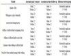
Table 1. Density functional theory (DFT) calculated graphene/hexagonal boron nitride heterojunction tight-binding modelof the nearest neighbor atomic transition energies in plane and interlayer and the in-situ potential energy of nitrogen and boron atoms [22] . The unit of medium energy is eV in the table
表1. 密度泛函理论(DFT)计算出的石墨烯/六方氮化硼异质结的紧束缚模型的面内和层间最近邻原子跃迁能以及氮原子和硼原子的在位势能 [22]。表中能量单位为eV
在本文中我们着重研究GBNNR的性质。GBNNR在一个方向可以无限延伸,而在另一个方向则是有限尺寸,同石墨烯纳米带一样,GBNNR也有两种特殊边缘构型,即锯齿型GBNNR (ZGBNNR)和扶手椅型GBNNR (AGBNNR)。我们分别计算了不同堆叠情况下两种不同边缘构型的GBNNR的能带结构,以此说明边缘构型对能带结构的影响。
从图2中我们可以清晰地看到,无论是ZGBNNR的能带结构还是AGBNNR的能带结构,都有能隙的打开,并且不同的堆叠方式导致能隙打开的程度也是不同的。
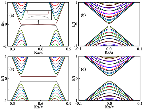
Figure 2. The band structures of GBNNR without potential field. (a) and (c) the band structure of AA-stackedand AB-stacked ZGBNNR without potential field. The inset shows the enlargement of band structure nearby the zero energy; (b) and (d) the band structure of AA-stackedand AB-stacked AGBNNR without potential field
图2. 无势场作用下GBNNR能带结构示意图。(a)和(c)为无势场作用下AA堆叠型和AB堆叠型ZGBNNR的能带结构。插图显示的是零能附近的能带放大图;(b)和(d)为无势场作用下AA堆叠型和AB堆叠型AGBNNR的能带结构
在本文中,我们将探究局域势和层间势对ZGBNNR和AGBNNR能带结构的影响。我们首先讨论在石墨烯层施加局域势时,能带结构变化情况。
对于AB堆叠型ZGBNNR,从图3(a)的相图中我们可以清晰地看到,通过调控V1和V2可以实现能隙由打开到闭合的变化,这表明异质结由绝缘相向金属相的转变。当V2处在0.4 eV附近时异质结的能隙始终为零。图3(b)中,当V1 = −0.30 eV,V2 = 0.20 eV时,异质结的能带是有能隙的,而图3(c)中,当V1 = −0.38 eV,V2 = 0.31 eV时,异质结的能带变成无能隙的。与AB堆叠型ZGBNNR相似,对于AA堆叠型ZGBNNR,从图3(d)的相图中我们可以发现,通过调控V1和V2可以也出现能隙的打开与闭合,进而实现绝缘相–金属相变。图3(e)和图3(f)显示当参数从V1 = −1.80 eV,V2 = −2.00 eV变到V1 = −1.90 eV,V2 = −1.10 eV时,异质结的能带是从有能隙变成无能隙。因此,根据上述分析我们可以知道,无论是AB堆叠型ZGBNNR还是AA堆叠型ZGBNNR,都可以通过调控局域势V1、V2来实现体系能带从零能隙向非零能隙的转变,即实现金属–绝缘体转变。
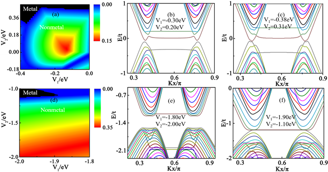
Figure 3. The phase diagrams and band structures of the AB-stacked and AA-stacked ZGBNNR under the local potentials. (a) The phase diagram of the energy gap of AB-stacked ZGBNNR as a function of V1 and V2. The gap of the black region is zero, suggesting a metallic phase; (b) and (c) the band structures of AB-stacked ZGBNNR before and after the energy gapis opened; (d)~(f) are similar to those of (a)~(c) but for AA-stacked ZGBNNR
图3. AB堆叠型和AA堆叠型ZGBNNR在局域势调控下的相图和能带结构。(a)表示AB堆叠型ZGBNNR的能隙随V1和V2变化的相图,图中黑色区域表示能隙为零,异质结处于金属相。(b)和(c)表示AB堆叠型ZGBNNR的能隙在打开前后的能带结构。(d)~(f)与(a)~(c)类似,但是属于AA堆叠型ZGBNNR的
如图4(a)和图4(b)所示,对于AB堆叠型和AA堆叠型AGBNNR,无论怎么调控局域势V1、V2,异质结的能带始终是有能隙的。因此,我们无法通过调控V1、V2来改变体系的能隙,从而实现相变。这一点与之前的ZGBNNR截然不同,这主要归因于两种纳米带边缘构型的差异:ZGBNNR在费米面附近存在局域化的近平带(如图2(a)中的插图),因此可以通过施加局域势调控这些局域化的近平带进而使能隙闭合;而AGBNNR没有这种特殊的局域态,自然无法像ZGBNNR那样通过局域势调控能隙。
对于AB堆叠型ZGBNNR,从图5(a)的相图中我们发现,通过调控U1和U2可以使异质结的能隙由打开变成闭合,实现异质结由绝缘相向金属相的转变。从图5(b)中参数U1 = −1.50 eV,U2 = −1.50 eV时,异质结的能带结构是有能隙的,而图5(c)中参数U1 = −1.50 eV,U2 = −0.10 eV时,异质结的能带结构是无能隙的。当U1 − U2 = −1.4 eV时,即沿着图5(a)中白色虚线方向能带是无能隙的且能级简并。从图5(d)~(f)的相图中我们可以发现,无论怎么调控U1、U2,异质结的能带结构始终是有能隙的。因此,对于AB堆叠型ZGBNNR,我们可以通过调控层间势U1、U2来实现体系从非零能隙向零能隙的转变,从而实现绝缘体–金属相变;但对于AA堆叠型ZGBNNR、AB堆叠型和AA堆叠型AGBNNR,我们无法通过调控U1、U2来使异质结的能隙闭合,也就不能实现相变。
Figure 4. The phase diagrams of the energy gap as a function of V1 and V2 for the (a) AB-stacked and (b) AA-stacked AGBNNR
图4. (a) AB堆叠型和(b) AA堆叠型AGBNNR的能隙随V1和V2变化的相图
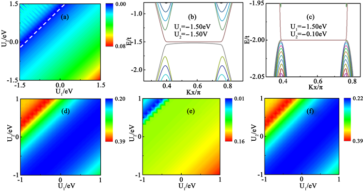
Figure 5. The phase diagrams and band structures of GBNNRs under the interlayer potentials. (a) A phase diagram of the energy gap of the AB-stacked ZGBNNR as a function of U1 and U2; (b) and (c) the corresponding band structures before and after an energy gap is opened; (d)~(f) the phase diagrams of the energy gap of the AA-stacked ZGBNNR, AB-stacked and AA-stacked AGBNNR as a function of U1 and U2, respectively
图5. GBNNR在层间势调控下的相图和能带结构。图(a)是AB堆叠型ZGBNNR能隙随U1和U2变化的相图;图(b)和(c)是能隙打开前后的能带结构。图(d)~(f)分别是AA堆叠型ZGBNNR,AB堆叠型和AA堆叠型AGBNNR能隙随U1和U2变化的相图
4. 结论
综上所述,我们用紧束缚模型研究了GBNNR的能带结构。我们发现无论是AB堆叠型还是AA堆叠型ZGBNNR的能带都可以由局域势单独调控,从而实现能隙的关闭和重新打开,即可以实现金属–绝缘体相变。而对于AB堆叠型ZGBNNR,我们仅可以通过层间势单独调控能带结构,使其能隙关闭和重新打开,即实现金属–绝缘体相变。这些结果为操纵石墨烯/h-BN异质结构的能带结构提供了一种简单而有效的方法。我们希望这些研究结果将有助于未来电子器件的开发和利用。
基金项目
本项目得到了国家自然科学基金项目(11864039)的资助。
文章引用
董记明,徐 雷,张 军. 势场调控下石墨烯/六方氮化硼范德瓦尔斯异质结的能带结构
Band Structure of Graphene/Hexagonal Boron Nitride Van Der Waals Heterojunction Manipulated by Potential Field[J]. 凝聚态物理学进展, 2021, 10(03): 73-79. https://doi.org/10.12677/CMP.2021.103009
参考文献
- 1. Castro, E.V., Novoselov, K.S., Morozov, S.V., et al. (2010) Electronic Properties of a Biased Graphenebilayer. Journal of Physics: Condensed Matter, 22, Article No. 175503. https://doi.org/10.1088/0953-8984/22/17/175503
- 2. Peres, N.M.R., Guinea, F. and Castro Neto, A.H. (2006) Electronic Properties of Disordered Two-Dimensional Carbon. Physical Review B, 73, Article No. 125411. https://doi.org/10.1103/PhysRevB.73.125411
- 3. Rao, C.N., Sood, A.K., Subrahmanyam, K.S., et al. (2009) Graphene: The New Two-Dimensional Nanomaterial. Angewandte Chemie International Edition, 48, 7752-7777. https://doi.org/10.1002/anie.200901678
- 4. Castro Neto, A.H., Guinea, F., Peres, N.M.R., et al. (2009) The Electronic Properties of Graphene. Reviews of Modern Physics, 81, 109-162. https://doi.org/10.1103/RevModPhys.81.109
- 5. Han, M.Y., Ozyilmaz, B., Zhang, Y., et al. (2007) Energy Band-Gap Engineering of Graphene Nanoribbons. Physical Review Letters, 98, Article No. 206805. https://doi.org/10.1103/PhysRevLett.98.206805
- 6. Yang, L., Park, C.H., Son, Y.W., et al. (2007) Quasiparticle Energies and Band Gaps in Graphene Nanoribbons. Physical Review Letters, 99, Article No. 186801. https://doi.org/10.1103/PhysRevLett.99.186801
- 7. Bostwick, A., Mcchesney, J., Ohta, T., et al. (2009) Experimental Studies of the Electronic Structure of Graphene. Progress in Surface Science, 84, 380-413. https://doi.org/10.1016/j.progsurf.2009.08.002
- 8. Castro, E.V., Novoselov, K.S., Morozov, S.V., et al. (2007) Biased Bilayer Graphene: Semiconductor with a Gap Tunable by the Electric Field Effect. Physical Review Letters, 99, Article No. 216802. https://doi.org/10.1103/PhysRevLett.99.216802
- 9. Moon, P. and Koshino, M. (2014) Electronic Properties of Graphene/Hexagonal-Boron-Nitride Moiré Superlattice. Physical Review B, 90, Article No. 155406. https://doi.org/10.1103/PhysRevB.90.155406
- 10. N’diaye, A.T., Bleikamp, S., Feibelman, P.J., et al. (2006) Two-Dimensional Ir Cluster Lattice on a Graphene Moire on Ir (111). Physical Review Letters, 97, Article No. 215501. https://doi.org/10.1103/PhysRevLett.97.215501
- 11. Varchon, F., Feng, R., Hass, J., et al. (2007) Electronic Structure of Epitaxial Graphene Layers on SiC: Effect of the Substrate. Physical Review Letters, 99, Article No. 126805. https://doi.org/10.1103/PhysRevLett.99.126805
- 12. Fan, Y., Zhao, M., Wang, Z., et al. (2011) Tunable Electronic Structures of Graphene/Boron Nitrideheterobilayers. Applied Physics Letters, 98, Article No. 083103. https://doi.org/10.1063/1.3556640
- 13. Titov, M. and Katsnelson, M.I. (2014) Metal-Insulator Transition in Graphene on Boron Nitride. Physical Review Letters, 113, Article No. 096801. https://doi.org/10.1103/PhysRevLett.113.096801
- 14. Watanabe, K., Taniguchi, T. and Kanda, H. (2004) Direct-Bandgap Properties and Evidence for Ultravioletlasing of Hexagonalboron Nitride Single Crystal. Nature Materials, 3, 404-409. https://doi.org/10.1038/nmat1134
- 15. Chittari, B.L., Chen, G., Zhang, Y., et al. (2019) Gate-Tunable Topological Flat Bands in TrilayerGraphene Boron-Nitride Moire Superlattices. Physical Review Letters, 122, Article No. 016401. https://doi.org/10.1103/PhysRevLett.122.016401
- 16. Song, J.C., Samutpraphoot, P. and Levitov, L.S. (2015) Topological Bloch Bands in Graphenesuperlattices. Proceedings of the National Academy of Sciences of the United States of America, 112, 10879-10883. https://doi.org/10.1073/pnas.1424760112
- 17. Yokomizo, Y. and Nakamura, J. (2013) Giant Seebeck Coefficient of the Graphene/h-BN Superlattices. Applied Physics Letters, 103, Article No. 113901. https://doi.org/10.1063/1.4820820
- 18. Jiang, Z., Henriksen, E.A., Tung, L.C., et al. (2007) Infrared Spectroscopy of Landau Levels of Graphene. Physical Review Letters, 98, Article No. 197403. https://doi.org/10.1103/PhysRevLett.98.197403
- 19. Jung, J., Dasilva, A.M., Macdonald, A.H., et al. (2015) Origin of Band Gaps in Graphene on Hexagonal Boron Nitride. Nature Communications, 6, Article No. 6308. https://doi.org/10.1038/ncomms7308
- 20. Wallbank, J.R., Patel, A.A., Mucha-Kruczyński, M., et al. (2013) Generic Miniband Structure of Graphene on a Hexagonal Substrate. Physical Review B, 87, Article No. 245408. https://doi.org/10.1103/PhysRevB.87.245408
- 21. Yankowitz, M., Xue, J., Cormode, D., et al. (2012) Emergence of Superlattice Dirac Points in Graphene on Hexagonal Boron Nitride. Nature Physics, 8, 382-386. https://doi.org/10.1038/nphys2272
- 22. Sławińska, J., Zasada, I., Kosiński, P., et al. (2010) Reversible Modifications of Linear Dispersion: Graphene between Boron Nitride Monolayers. Physical Review B, 82, Article No. 085431. https://doi.org/10.1103/PhysRevB.82.085431
NOTES
*通讯作者。