Advances in Material Chemistry
Vol.04 No.03(2016), Article ID:17977,9
pages
10.12677/AMC.2016.43003
Fabrication and Optical-Electrical Properties of P-Type Manganese-Doped Titanium Dioxide Nano-Films
Peizhan Liu, Xiaohong Xia*, Yun Gao
Faculty of Materials Science and Engineering, Hubei University, Wuhan Hubei

Received: Jun. 23rd, 2016; accepted: Jul. 10th, 2016; published: Jul. 13th, 2016
Copyright © 2016 by authors and Hans Publishers Inc.
This work is licensed under the Creative Commons Attribution International License (CC BY).
http://creativecommons.org/licenses/by/4.0/


ABSTRACT
Manganese, as a 3d transition metal element, is considered to be one of the potential dopants for TiO2 to adjust the optical-electrical properties of TiO2, aiming to improve the utilization of sunlight, conductivity and carrier mobility of TiO2. The modified TiO2 could then be widely used in the intelligent photo-catalytic, semiconductor sensors, solar cells, etc. In this paper, we have prepared p-type Manganese-doped TiO2 rutile nano-film on amorphous silica/quartz substrates by radio frequency magnetron sputtering method with a Mn0.8Ti1.2O3 solid ceramic target. XRD, EDS, AFM, XPS, UV-Vis-IR, Two-Probe and Hall effect measurements were used to investigate the influences of Mn doping on the crystalline structure, surface state, optical and electrical properties of TiO2 nano-film. The results have shown that Mn doping could effectively extend the light absorption region of TiO2 from UV to visible light. The doping ratio was tuned by adjusting the sputtering power, the higher the sputtering power, the bigger ratio Mn was doped into TiO2. Electrical conductivity of the thin films increased with increase of Mn doping ratio. Mn precipitated when the sputtering power for Mn0.8Ti1.2O3 reached 150 W, suggesting that there is incorporation limit for Mn in TiO2 lattice. The P type Mn doped TiO2 could be used in various applications such as solar cell, gas sensors and photosplitting of water.
Keywords:Mn Doping, Magnetron Sputtering, Titanium Dioxide, Optical and Electrical Properties

P型Mn掺杂TiO2纳米薄膜的制备及其光电性能研究
刘培战,夏晓红*,高云
湖北大学材料科学与工程学院,湖北 武汉

收稿日期:2016年6月23日;录用日期:2016年7月10日;发布日期:2016年7月13日

摘 要
采用射频磁控溅射法以Mn0.8Ti1.2O3固相陶瓷靶为靶材,在石英衬底上制备了Mn掺杂TiO2纳米薄膜,通过XRD、EDS、AFM、XPS、UV-Vis-IR、两探针法和半导体霍尔效应等测试表征技术研究了Mn掺杂对TiO2薄膜的晶体结构、表面化学态和光电性能的影响。结果表明,Mn掺杂TiO2薄膜为p型半导体,随着溅射功率的增加,薄膜的光吸收向可见光方向移动,电导率增加。过量Mn掺杂会导致Mn元素的析出,光吸收性能和电学性能均变差,说明Mn掺杂是TiO2薄膜光电性能改善的根本原因。
关键词 :Mn掺杂,磁控溅射,TiO2,光电性能

1. 引言
自1972年Fujishima和Honda采用TiO2半导体电极成功实现催化分解水以来 [1] ,有关TiO2纳米材料光学 [2] 、电学 [3] 和磁学 [4] 性能的研究逐步引起了科学界的广泛关注。TiO2作为一种宽禁带(锐钛矿相~3.2 eV、金红石相~3.0 eV)n型半导体材料 [5] ,因其独特的结构和稳定的性能被广泛应用于智能光催化 [6] [7] 、太阳能电池 [8] [9] 、半导体传感器 [10] 、超级电容器 [11] 、功能陶瓷 [12] 、空气净化 [13] 等领域。然而,本征TiO2的太阳光利用率较低,光吸收范围对应于太阳光谱中的紫外光区,无法有效利用可见光及近红外光区 [14] ;同时,本征TiO2的电导率和载流子迁移率都很低,不利于光生载流子的传输,TiO2的应用前景受限。对TiO2进行掺杂或缺陷态调控可有效调节TiO2的能带结构,改善其光电性能。Alberto等通过一步结晶法获得了带隙显著减小、光响应范围拓宽到可见光区的黑色TiO2纳米颗粒,并详细研究了缺陷的性质和位置对带隙窄化的影响机制 [15] 。然而,大量缺陷的存在对于载流子传输极为不利,在传输过程中极易发生电子-空穴对的复合,载流子的寿命较短。掺杂被认为是调控TiO2带隙的最有效的方法之一,典型的非金属掺杂有C [16] 、N [17] 、F [18] 、P [19] 、S [20] 等,金属掺杂有Mn [21] 、Fe [22] 、Nb [23] 、Zn [24] 、Cr [25] 、Co [26] 、Nd [27] 、Er [28] 、V [29] 、Ag [30] 、Sr [31] 等,通过这些离子掺杂可有效提升TiO2的可见光吸收能力的 [32] ,改善TiO2薄膜的光学和电学性能 [33] 。
目前,关于TiO2的n型掺杂已取得较大进展,如Nb掺杂TiO2薄膜已成功应用于透明导电薄膜 [23] ,而TiO2的p型掺杂还处于起步阶段 [34] ,面临的困难较大,主要阻碍来源于p型掺杂的TiO2稳定性不佳。解决这一问题的关键在于制备高质量的、有效掺杂的纳米薄膜。我们前期在第一性原理计算 [35] 的指导下,已用水热法制备了Mn掺杂TiO2粉体材料 [36] ,掺杂薄膜的光吸收及光催化性能明显改善;还用磁控溅射法制备了p型Mn掺杂TiO2薄膜,掺杂后薄膜的电学性能明显提升 [5] [21] 。为克服前期研究工作中采用的Mn金属靶易碎,所制备的薄膜易被污染、性能不稳定等问题,本文采用射频磁控溅射法以Mn0.8Ti1.2O3固相陶瓷靶为靶材制备p型Mn掺杂TiO2纳米薄膜,研究射频功率对薄膜的结构、形貌、光吸收性能和电学性能的影响。
2. 实验部分
2.1. 薄膜的制备
采用射频磁控溅射法(中科院沈科仪JPG-400型超高真空磁控溅射沉积系统),以高纯钛酸锰固相陶瓷靶(Mn0.8Ti1.2O3,纯度99.999%,直径50.8 mm,厚度3 mm)为靶材,以石英玻璃(20 mm × 20 mm × 1 mm)为衬底,真空度优于2.0 × 10⁻⁴ Pa,靶材与衬底间距保持为50 mm,衬底温度为500℃,工作压强为0.5 Pa,Ar气体流量为50 sccm,O2气体流量为0.7 sccm,预溅射时间为15 min,溅射时间为2 h,射频溅射功率分别为30 W、60 W、90 W、120 W和150 W制备Mn掺杂TiO2纳米薄膜。溅射前将石英玻璃衬底依次置于盛有丙酮(AR)、无水乙醇(AR)和去离子水的烧杯中采用数控超声波清洗器(KQ-250DB)进行超声清洗20 min,以充分除去石英衬底表面可能存在的污染物。将洗净的石英玻璃衬底用电热恒温干燥箱(202-0AB)烘干后固定于样品托上,将靶材和样品托装配至指定位置并进行抽真空、衬底加热、预溅射和溅射沉积等过程。将溅射功率为30 W、60 W、90 W、120 W和150 W制备的薄膜样品依次标号为S1、S2、S3、S4和S5。
2.2. 薄膜的测试表征
采用EDS(Oxford,X-Max 50)在局部区域扫描以确定薄膜样品中的元素组成及百分比含量,采用XRD (Bruker, D8A25)在2θ扫描模式下选用Cu-Kα辐射源(波长0.15406 nm,光管电压50 kV,电流20 mA,扫描范围20˚~70˚,扫描速率5˚/min)确定薄膜样品的晶体结构及物相,采用AFM (NT-MDT, Solver Nano)在半接触模式下选用NSG01_Ed及FMG01/Pt针尖确定薄膜样品的显微形貌、平均表面粗糙度及膜厚,采用XPS (Thermo Fisher, ESCALAB 250)进行全谱、窄谱和价带谱扫描以确定薄膜样品表面的Mn、Ti原子百分比含量、化学价态和价带分布情况,采用UV-Vis-IR(Shimadzu, UV-3600)在直接扫描模式下选用狭缝宽度5.0,波长扫描范围300 nm~1500 nm,扫描间隔1 nm进行薄膜样品的光学性能分析,采用半导体测试两探针法(Keithley, 4200)在I~V特性模式下选用电压扫描范围−5 V~5 V,间隔0.05 V进行薄膜样品的电阻率和方块电阻等电学性能分析,采用半导体霍尔效应(Ecopia, HMS-3000)测试确定薄膜样品的导电类型、载流子浓度和迁移率等电学性能参数。
3. 结果与讨论
3.1. 薄膜的晶体结构及组成分析
图1为S1~S5的XRD图谱,与标准PDF卡片对比后发现S1~S4中均出现金红石型TiO2(110)衍射峰,并且(110)衍射峰的半高宽随着溅射功率的增大逐渐减小,说明薄膜样品的晶粒尺寸变大,根据谢乐公式计算出S1~S4的平均晶粒尺寸分别为8.2 nm、8.7 nm、9.5 nm和11.2 nm。S5样品中R(110)峰较弱,出现较强的MnO2和Mn2O3衍射峰,说明150 W的溅射功率下Mn元素发生了析出。在S5中Mn元素析出后R(110)的位置与标准卡位置一致,而S1~S4中R(110)峰位均有一定程度右移,右移幅度△θ在0.35˚~0.5˚之间且随着功率的增大而减小,说明S1~S4中Mn元素的掺杂引起了TiO2的晶格改变。Mn和Ti的离子半径分别为:Mn2+(0.67Å)、Mn3+(HS 0.645Å、LS 0.58 Å)、Mn4+(0.53Å)、Ti4+(0.605Å)、Ti3+(0.67Å),Mn3+、
Mn4+离子半径比Ti4+、Ti3+要小,Mn元素的掺杂导致TiO2的晶胞参数和晶面间距变小,根据Bragg定律2dsinθ = nλ,衍射角增大衍射峰峰位右移。S5样品中Mn元素部分析出后,其对TiO2晶格的影响减小,(110)衍射峰回到标准峰位。
表1为不同溅射功率下制备的薄膜样品S1~S5的EDS测试结果,与实验用Mn0.8Ti1.2O3固相陶瓷靶材对比后发现,薄膜样品S1中Mn原子的相对含量比靶材中的40.0 at.%略大,S2~S5中Mn、Ti原子的相对含量均比靶材中的高且呈逐渐增大的趋势,主要原因是在陶瓷靶的溅射过程中Mn的溅射产额比Ti大。
3.2. 薄膜表面形貌及膜厚分析(AFM)
图2为不同溅射功率下制备的掺杂薄膜样品S1~S4的AFM表面形貌图,从图中可以看出:薄膜样品的平均晶粒尺寸随溅射功率增大逐渐增大,与XRD结果一致。薄膜样品的表面光滑、致密,表面粗糙度均方根Sq在1 nm~3 nm、平均表面粗糙度Sa在1 nm~2 nm。在薄膜边缘制造台阶用AFM检测薄膜S1~S4的厚度约为400 nm,S5的膜厚略小,为340 nm左右。
3.3. 薄膜的表面元素价态及价带位置分析(XPS)
图3为不同溅射功率下制备的Mn掺杂TiO2纳米薄膜样品S1~S4经过C1s (284.8 eV)校准后的XPS图谱。图3(a)为Ti 2p图谱,从图中可以看出:Ti 2p1/2和Ti 2p3/2对应的峰位分别在463.1 eV和457.4 eV

Figure 1. The XRD patterns of sample S1 - S5
图1. 样品S1~S5的XRD图谱
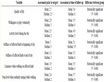
Table 1. The EDS test results of sample S1 - S5
表1. 样品S1~S5的EDS测试结果

Figure 2. AFM surface morphology images of sample S1 - S4
图2. 掺杂薄膜样品S1~S4的AFM表面形貌图
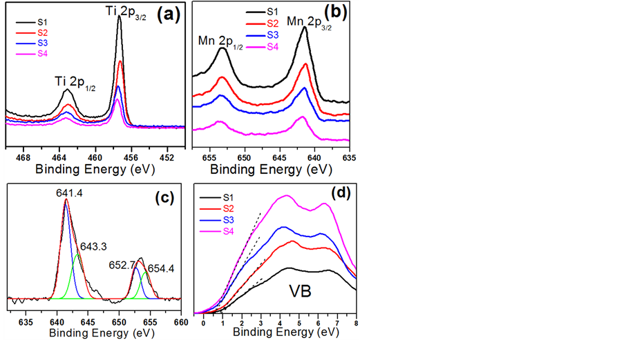
Figure 3. XPS spectra of samples S1 - S4:(a) Ti 2p; (b) Mn 2p; (c) Mn 2p fitting; (d) valence band
图3. 样品S1~S4的XPS图谱:(a) Ti 2p;(b) Mn 2p;(c) Mn 2p分峰;(d) 价带谱
且峰距△EB.E. ≈ 5.7 eV,表明Ti在薄膜中呈现为+4价 [37] 。随着溅射功率的增大结合能向高能方向略有偏移,说明Mn掺杂导致电子云偏离Ti原子核。图3(b)为Mn的XPS图谱,从图中可以看出:Mn 2p1/2和Mn 2p3/2明显宽化,可拟合成两组单峰,如图3(c)所示。两组峰的峰位分别在652.7 eV和641.4 eV以及654.4eV和643.3eV,对应于Mn3+和Mn4+,说明Mn元素在薄膜中以+3和+4价存在,与我们前期的实验结果一致 [5] [36] 。图3(d)是掺杂样品的价带谱,从图中可以看出,随着溅射功率的增大,即Mn含量的增加,价带顶上移,说明Mn元素掺杂使得TiO2的带隙变窄,且以p型掺杂的形式进入TiO2晶格进行掺杂。
样品S1~S5的光吸收特性用紫外可见红外吸收光谱表征,如图4所示。在可见和红外波段,样品S2~S4有明显的干涉峰,而样品S1和S5均未形成的明显的干涉峰。干涉峰的出现主要由两方面的原因引起,一是样品的厚度,从AFM表征结果看,S5的厚度偏小,因而在吸收光谱中没有出现干涉峰,二是样品对光的吸收,S1样品中Mn掺杂含量较低,对TiO2的光吸收效应较小,亦未出现干涉峰。对于样品S1~S4,随着Mn掺杂含量的增加,样品的吸收带边向可见光方向移动,薄膜样品S1~S5均呈棕褐色,且颜色逐渐加深。通过Tauc公式αhv = K(hv-Eg)n (直接带隙n = 2)计算得到样品S1~S5的带隙分别为:2.61 eV,2.32 eV,2.22 eV,1.91 eV和2.76eV,S1-S4随着掺杂浓度增加带隙逐渐减小,S5由于Mn元素的部分析出带隙比S1~S4大,但是比纯金红石型TiO2 (3.0eV)小。
3.4. 薄膜的电学性能分析
采用Keithley 4200型半导体测试仪和两探针法,考虑薄膜的电阻率为ρ、膜厚t、电极宽度w、接触电阻为Rc等因素,测试薄膜的I~V特性直线,采用线性拟合的方式扣除接触电阻,计算薄膜的方块电阻、电阻率和电导率,结果如表2所示。从表中可以看出,薄膜样品S1~S4的方块电阻随着溅射功率的增大而减小、电导率随着溅射功率的增大而增大,比纯TiO2 (10−6 Ω−1∙cm−1)提升了四个数量级。薄膜样品S5在测试时超出了量程,主要是由于Mn原子在TiO2中析出,电阻增大。

Figure 4. UV-Vis-IR spectra of sample S1 - S5
图4. 样品S1~S5的UV-Vis-IR图谱
Table 2. Electrical properties test results of sample S1 - S5
表2. 薄膜样品S1~S5的电学性能测试结果
此外,我们还对薄膜样品S4进行了霍尔效应测试,结果表明:薄膜样品S4的导电类型为p型,霍尔迁移率μH = 1.14102 × 10⁻⁶ m²/V∙s、载流子浓度n = 1.53686 × 1025 m-3、霍尔系数RH = 4.06122 × 10⁻⁷ m³/C、电阻率ρ = 0.455928723 Ω·m、方块电阻R = 5898218.064 Ω,与用半导体参数测试仪测试的结果基本一致。
过渡金属元素Mn被认为是最有潜力的p型掺杂剂之一,主要优势在于:(1) 离子半径接近Ti4+,Mn掺杂可使Mn4+或Mn3+离子部分替代Ti4+以精细调制TiO2的电子或能带结构;(2) Mn掺杂可有效提升TiO2的可见光响应、拓宽其光吸收范围;(3) Mn掺杂可引入中间能级,成为电子从价带跃迁到导带的跳板,促进电荷的分离并有效地阻止电荷复合,促进光生载流子的传输,改善电学性能。
4. 结论
本文研究了溅射功率对Mn掺杂TiO2纳米薄膜的晶体结构、表面形貌、元素价态和光电性能的影响。结果表明:随着溅射功率的增大,薄膜中的Mn百分比含量逐渐增大,功率过大会导致Mn元素析出。Mn掺杂含量的增加有利于改善薄膜的质量、减小表面粗糙度,Mn掺杂拓宽了TiO2薄膜的光响应范围,掺杂薄膜的光吸收带边发生显著红移,表现出p型导电特性,且薄膜的电导率随Mn含量的增加而增大。Mn含量在48.2at.%~49.8at%之间可得到薄膜质量和光电性能较好的TiO2薄膜,过量Mn掺杂导致薄膜光吸收和电学性能的退化,表明Mn掺杂是TiO2薄膜光电性能改善的根本原因。
基金项目
感谢国家自然科学基金(批准号:11374091,11004051,11274100),国家教育部基金(批准号:211108,20134208110005)和湖北省科技厅(批准号:2011BAB032)项目的支持。
文章引用
刘培战,夏晓红,高 云. P型Mn掺杂TiO2纳米薄膜的制备及其光电性能研究
Fabrication and Optical-Electrical Properties of P-Type Manganese-Doped Titanium Dioxide Nano-Films[J]. 材料化学前沿, 2016, 04(03): 21-29. http://dx.doi.org/10.12677/AMC.2016.43003
参考文献 (References)
- 1. Fujishima, A. and Honda, K. (1972) Electrochemical Photolysis of Water at a Semiconductor Electrode. Nature, 238, 37-38. http://dx.doi.org/10.1038/238037a0
- 2. Mazur, M., Wojcieszak, D., Kaczmarek, D., et al. (2015) Effect of the Nanocrystalline Structure Type on the Optical Properties of TiO2:Nd (1at.%) thin films. Optical Materials, 42, 423-429. http://dx.doi.org/10.1016/j.optmat.2015.01.040
- 3. Nkosi, S.S., Kortidis, I., Motaung, D.E., et al. (2014) An Instant Pho-to-Excited Electrons Relaxation on the Photo-Degradation Properties of TiO2−x Films. Journal of Photochemistry and Photobiology A: Chemistry, 293, 72-80. http://dx.doi.org/10.1016/j.jphotochem.2014.07.012
- 4. Patel, S.K.S., Gajbhiye, N.S. and Date, S.K. (2011) Ferromagnetism of Mn-Doped TiO2 Nanorods Synthesized by Hydrothermal Method. Journal of Alloys and Compounds, 509, S427-S430. http://dx.doi.org/10.1016/j.jallcom.2011.01.086
- 5. Xia, X.H., Lu, L., Walton, A.S., et al. (2012) Origin of Significant Visi-ble-Light Absorption Properties of Mn-Doped TiO2 Thin Films. Acta Materialia, 60, 1974-1985. http://dx.doi.org/10.1016/j.actamat.2012.01.006
- 6. Fujishima, A., Rao, T.N. and Tryk, D.A. (2000) Titanium Dioxide Photo-catalysis. Journal of Photochemistry and Photobiology C: Photochemistry Reviews, 1, 1-2. http://dx.doi.org/10.1016/S1389-5567(00)00002-2
- 7. Yu Y., Wang, J., Parr J.F., et al. (2012) Preparation and Properties of TiO2/Fumed Silica Composite Photocatalytic Materials. Procedia Engineering, 27, 448-456. http://dx.doi.org/10.1016/j.proeng.2011.12.473
- 8. Kim, D.H., Han, G.S., Seong, W.M., et al. (2015) Niobium Doping Effects on TiO2 Mesoscopic Electron Transport Layer-Based Perovskite Solar Cells. ChemSusChem, 8, 2392-2398. http://dx.doi.org/10.1002/cssc.201403478
- 9. Bao, N., Feng, X. and Grimes, C.A. (2012) Self-Organized One-Dimensional TiO2 Nanotube/Nanowire Array Films for Use in Excitonic Solar Cells: A Review. Journal of Nanotechnology, 2012, 1-27. http://dx.doi.org/10.1155/2012/645931
- 10. Ojani, R., Safshekan, S. and Raoof, J.B. (2013) Photoelectrochemical Oxidation of Hydrazine on TiO2 Modified Titanium Electrode: Its Application for Detection of Hydrazine. Journal of Solid State Electrochemistry, 18, 779-783. http://dx.doi.org/10.1007/s10008-013-2321-y
- 11. Trenczek-Zajac, A., Pamula, E., Radecka, M., et al. (2012) Thin Films of TiO2:N for Photo-Electrochemical Applications. Journal of Nanoscience and Nanotechnology, 12, 4703-4709. http://dx.doi.org/10.1166/jnn.2012.4937
- 12. Chao, S. and Dogan, F. (2011) Effects of Manganese Doping on the Dielectric Properties of Titanium Dioxide Ceramics. Journal of the American Ceramic Society, 94, 179-186. http://dx.doi.org/10.1111/j.1551-2916.2010.04039.x
- 13. Novotná, P., Zita, J., Krýsa, J., et al. (2008) Two-Component Trans-parent TiO2/SiO2 and TiO2/PDMS Films as Efficient Photocatalysts for Environmental Cleaning. Applied Catalysis B: Environmental, 79, 179-185. http://dx.doi.org/10.1016/j.apcatb.2007.10.012
- 14. Chen X.B. and Mao. S.S. (2007) Titanium Dioxide Nanomaterials: Synthesis, Properties, Modifications, and Applications. Chemical Reviews, 107, 2891-2959. http://dx.doi.org/10.1021/cr0500535
- 15. Naldoni, A., Allieta, M., Santangelo, S., et al. (2012) Effect of Nature and Location of Defects on Bandgap Narrowing in Black TiO2 Nanoparticles. Journal of the American Chemical Society, 134, 7600-7603. http://dx.doi.org/10.1021/ja3012676
- 16. Dang, B.H.Q., Rahman, M., MacElroy, D. and Dowling, D.P. (2012) Evaluation of Microwave Plasma Oxidation Treatments for the Fabrication of Photoactive Un-Doped and Carbon-Doped TiO2 Coatings. Surface and Coatings Technology, 206, 4113-4118. http://dx.doi.org/10.1016/j.surfcoat.2012.04.003
- 17. Lee, S.H., Yamasue, E., Okumura, H. and Ishihara, K.N. (2015) Effect of Substrate Roughness and Working Pressure on Photocatalyst of N-Doped TiOx Films Prepared by Reactive Sputtering with Air. Applied Surface Science, 324, 339- 348. http://dx.doi.org/10.1016/j.apsusc.2014.10.173
- 18. Li, B.J., Huang, L.J., Ren, N.F. and Zhou, M. (2014) Titanium Dioxide-Coated Fluorine-Doped Tin Oxide Thin Films for Improving Overall Photoelectric Property. Applied Surface Science, 290, 80-85. http://dx.doi.org/10.1016/j.apsusc.2013.11.001
- 19. Comsup, N., Panpranot, J. and Praserthdam, P. (2010) The Effect of Phos-phorous Precursor on the CO Oxidation Activity of P-Modified TiO2 Supported Ag Catalysts. Catalysis Communications, 11, 1238-1243. http://dx.doi.org/10.1016/j.catcom.2010.06.014
- 20. Wang, Y.P., Li, J., Peng, P., Lu, T.H. and Wang, L.J. (2008) Preparation of S-TiO2 Photocatalyst and Photodegradation of L-Acid under Visible Light. Applied Surface Science, 254, 5276-5280. http://dx.doi.org/10.1016/j.apsusc.2008.02.050
- 21. Lu, L., Xia, X.H., Luo, J.K. and Shao, G. (2012) Mn-Doped TiO2 Thin Films with Significantly Improved Optical and Electrical Properties. Journal of Physics D: Applied Physics, 45, 485102. http://dx.doi.org/10.1088/0022-3727/45/48/485102
- 22. Nair, P.B., Justinvictor, V.B., Daniel, G.P., et al. (2014) Structural, Optical, Photoluminescence and Photocatalytic Investigations on Fe Doped TiO2 Thin Films. Thin Solid Films, 550, 121-127. http://dx.doi.org/10.1016/j.tsf.2013.10.112
- 23. Castro, M.V., Rebouta, L., Alpuim, P., et al. (2014) Optimisation of Surface Treatments of TiO2:Nb Transparent Conductive Coatings by a Post-Hot-Wire Annealing in a Reducing H2 Atmosphere. Thin Solid Films, 550, 404-412. http://dx.doi.org/10.1016/j.tsf.2013.11.044
- 24. Jing, L.Q., Xin, B.F., Yuan, F.L., Xue, L.P., Wang, B.Q. and Fu, H.G. (2006) Effects of Surface Oxygen Vacancies on Photophysical and Photochemical Processes of Zn-Doped TiO2 Nanoparticles and Their Relationships. The Journal of Physical Chemistry B, 110, 17860-17865. http://dx.doi.org/10.1021/jp063148z
- 25. Hajjaji, A., Atyaoui, A., Trabelsi, K., et al. (2014) Cr-Doped TiO2 Thin Films Prepared by Means of a Magnetron Co-Sputtering Process: Photo-catalytic Application. American Journal of Analytical Chemistry, 5, 473-482. http://dx.doi.org/10.4236/ajac.2014.58056
- 26. Buha, J. (2013) Photoluminescence Study of Carbon Doped and Hydrogen Co-Doped TiO2 Thin Films. Thin Solid Films, 545, 234-240. http://dx.doi.org/10.1016/j.tsf.2013.08.049
- 27. Ali, A., Yassitepe, E., Ruzybayev, I., Shah, S.I. and Bhatti, A.S. (2012) Improvement of (004) Texturing by Slow Growth of Nd Doped TiO2 Films. Journal of Applied Physics, 112, 113505. http://dx.doi.org/10.1063/1.4767361
- 28. Johannsen, S.R., Lauridsen, L.R., Julsgaard, B., Neuvonen, P.T., Rama, S.K. and Larsen, A.N. (2014) Optimization of Er3+-Doped TiO2-Thin Films for Infrared Light Up-Conversion. Thin Solid Films, 550, 499-503. http://dx.doi.org/10.1016/j.tsf.2013.10.123
- 29. Yildirim, O., Butterling, M., Cornelius, S., et al. (2014) Ferromagnetism and Structural Defects in V-Doped Titanium Dioxide. Physica Status Solidi (c), 11, 1106-1109. http://dx.doi.org/10.1002/pssc.201300722
- 30. Sornsanit, K., Horprathum, M., Chananonnawathorn, C., et al. (2013) Fabrication and Characterization of Antibacterial Ag-TiO2 Thin Films Prepared by DC Magnetron Co-Sputtering Technique. Advanced Materials Research, 770, 221- 224. http://dx.doi.org/10.4028/www.scientific.net/AMR.770.221
- 31. Hamedani, H.A., Allam, N.K., El-Sayed, M.A., Khaleel, M.A., Garmestani, H. and Alamgir, F.M. (2014) An Experimental Insight into the Structural and Electronic Characteristics of Strontium-Doped Titanium Dioxide Nanotube Arrays. Advanced Functional Materials, 24, 6783-6796. http://dx.doi.org/10.1002/adfm.201401760
- 32. Matsumoto, Y., Katayama, M., Takatoshi, A.B.E., et al. (2010) Chemical Trend of Fermi-Level Shift in Transition Metal-Doped TiO2 Film. Journal of the Ceramic Society of Japan, 118, 993-996. http://dx.doi.org/10.2109/jcersj2.118.993
- 33. Tsutomu, U., Tetsuya, Y., Hisayoshi I. and Keisuke, A. (2002) Analysis of Elec-tronic Structure of 3d Transition Metal-Doped TiO2 Based on Band Calculations. Journal of Physics and Chemistry of Solids, 63, 1909-1920. http://dx.doi.org/10.1016/S0022-3697(02)00177-4
- 34. Li, X., Wu, S., Hu, P., et al. (2009) Structures and Magnetic Properties of P-Type Mn:TiO2 Dilute Magnetic Semiconductor Thin Films. Journal of Applied Physics, 106, 043913. http://dx.doi.org/10.1063/1.3204493
- 35. Shao, G. (2008) Electronic Structures of Manganese-Doped Rutile TiO2 from First Principles. The Journal of Physical Chemistry C, 112, 18677-18685. http://dx.doi.org/10.1021/jp8043797
- 36. Deng, Q.R., Xia, X.H., Guo, M.L., Gao, Y. and Shao, G. (2011) Mn-Doped TiO2 Nanopowders with Remarkable Visible Light Photocatalytic Activity. Materials Letters, 65, 2051-2054. http://dx.doi.org/10.1016/j.matlet.2011.04.010
- 37. Moudler, J.F., Stickle, W.F., Sobol P.E., et al. (1992) Handbook of X-Ray Photoelectron Spectroscopy. Perkin-Elmer, Eden Prairie.