Material Sciences
Vol.06 No.03(2016), Article ID:17738,7
pages
10.12677/MS.2016.63026
Density Functional Theory Research of the Electronic Structure of Armchair Type Multi-Walled Silicon Nanotubes
Denghui Liu, Yuchao Tang, Chengpeng Yao, Hengjiang Zhu*
College of Physics and Electronic Engineering, Xinjiang Normal University, Urumqi Xinjiang

Received: May 8th, 2016; accepted: May 28th, 2016; published: May 31st, 2016
Copyright © 2016 by authors and Hans Publishers Inc.
This work is licensed under the Creative Commons Attribution International License (CC BY).
http://creativecommons.org/licenses/by/4.0/


ABSTRACT
One dimensional silicon nanomaterials with its unique optical, electrical and semiconductor properties attract widespread international attention. It has become one of the hot topics in the research of scientists. Silicon nanotubes in transistors, nano-electronic devices, sensors, field emission display devices, nano-magnetic devices and optoelectronic devices, hydrogen storage and electrochemical field have a broad application prospect. Because silicon is easy to form a linear structure of SP3 hybridization, silicon nanotubes synthesis is difficult. At present, silicon nanotubes research is still in initial stage. In this paper, we use the density functional theory to optimize the structure and calculate the frequency of the triple-wall silicon nanotubes, obtain the electronic properties, and conclude the property that the band gap decreases with the increase of the size.
Keywords:Silicon Nanotubes, Density Functional Theory, Structural Optimization, Band Gap

扶手椅型多壁硅纳米管电子特性的密度泛函理论研究
刘登辉,唐宇超,姚程鹏,祝恒江*
新疆师范大学物理与电子工程学院,新疆 乌鲁木齐

收稿日期:2016年5月8日;录用日期:2016年5月28日;发布日期:2016年5月31日

摘 要
一维硅纳米材料以其特有的光学、电学和半导体特性受到国际上广泛的关注,现已成为纳米科学家研究的热点之一。硅纳米管在晶体管等纳米电子器件、传感器、场发射显示器件、纳米磁性器件及光电器件、储氢及电化学等领域有着广阔的应用前景。由于硅元素为易于形成线状结构的SP3杂化,硅纳米管的制备合成比较困难,目前硅纳米管的研究依然处于初期阶段。本文采用密度泛函理论对三壁硅纳米管进行结构优化和频率计算,获得其电子性质,并得出了其带隙随着尺寸的增加而逐渐减小的性质。
关键词 :硅纳米管,密度泛函理论,结构优化,带隙

1. 引言
自从碳纳米管 [1] 和硅纳米管 [2] 等一维纳米材料被成功合成后,立即引起了诸多领域科学家的极大关注和浓厚兴趣 [3] - [7] ,一维纳米材料的研究成为了当今基础和应用研究的热点 [8] - [10] 。一维半导体材料具有与体材料截然不同的特殊性质 [11] [12] 。硅是间接带隙半导体,带隙窄,不适合光电器件的应用 [13] 。因此,硅在制备纳米器件是存在局限性,而多孔硅、硅纳米线的研究表明硅纳米材料可能在未来的纳米电子器件中具有很大的应用潜力。
由于硅和碳的π键结合能力不同,使其拥有了不同的化学性质。碳的S轨道和P轨道的能量差是硅的近两倍,所以硅是SP3杂化。碳较大的杂化能量说明其P轨道较活跃,所以碳具有较稳定的SP、SP2及SP3杂化。由于硅原子间距大于碳原子间距,硅的 键结合能力减少了一个数量级,导致了硅的 键结合能力远远低于碳的π键结合能力,所以碳容易形成石墨管状结构,而硅更易于形成类金刚石线状结构,所以长期以来对于一维硅纳米材料的研究仅限于硅纳米线方面,而对于硅纳米管理论研究成果多于实验成果。很多研究者提出了不同的模型说明在一定条件下硅纳米管可以稳定的存在,所以硅纳米管的研究目前已成为国际上研究的热点之一。
近些年,随着科学技术的发展,硅纳米管和硅纳米线成为在未来纳米电子器件领域中很有希望的应用纳米材料,硅纳米管收到了极大的关注,但与此同时,很多人质疑硅纳米管是否存在,直到Sha [14] 和Jeong在实验上成功合成硅纳米管。Fagan [15] 通过计算SP2型硅纳米管得出纳米管的带隙由纳米管的类型决定,Bai [16] 研究了零带隙SP3型硅纳米管。Zhang [17] 研究了小直径的单壁硅纳米管(SWS iNTs)的导电性能,与单壁碳纳米管 [18] [19] 一样它只有半导体导电性;并用B3LYP/6-31G (d)研究了三种有限的硅纳米管结构,他们预言了扶手性硅纳米管比锯齿型的硅纳米管更稳定。Zhang等人用半经验分子轨道的PM3方法计算了硅纳米管Si54H12,并用H F/3-21G和HF/3-21G(d)方法进行了验证 [20] 。结果表明:若管状结构两端的悬键被正常终止,原理上可形成表面有皱褶的硅纳米管。Barnardand Russo [21] 研究了无限长扶手型和锯齿型硅纳米管的能量和结构性质随管径的变化规律;Singh [22] 研究了掺杂金属的硅纳米管;Chen [23] 研究了悬氢单双壁硅纳米管的性质;所有这些理论和实验的研究表明,硅纳米管特性的研究存在重大的争议。
据查阅大量文献所知,对于多壁硅纳米管的研究很少,三壁硅纳米管的研究就更少了;通过文献和本文的研究可以得出,硅纳米管的带隙随着管壁数的增加而减小。
2. 模型及计算方法
图1中展示的是本文中所要研究的模型之一(即(4,4)@(8,8)@(12,12)型硅纳米管)的鸟瞰图和俯视图。本文所有多壁硅纳米管的几何构型优化和电子结构计算都使用了Gaussian03 [24] 软件包中的密度泛函理论(DFT)。基于DFT 的B3LYP [25] [26] 方法被用来描述交换–关联势。为了更好地描述无限长硅纳米管的几何特征和电子结构、全电子基组LanL2DZ [27] - [29] 被选择。全部优化过程是基于能量系统的收敛,其收敛的标准是1 × 10⁻⁶ a.u.。在构建模型的基础上,我们使用上述理论方法与周期性边界条件(PBC) [30] 来对多壁硅纳米管的几何结构和电子特性进行优化和计算。PBC模型是基于高斯型轨道(GTO) [31] ,此轨道是采用布洛赫函数变换的“结晶轨道(CO)” [32] 。最后,所有的单、多壁硅纳米管的能带结构计算均选取241个k点。
3. 计算结果与讨论
3.1. 多壁硅纳米管的结合能
多壁纳米管首先通过几何优化得到相对稳定的初始构型,然后通过频率计算以及消虚频等得到多壁纳米管的结合能和部分电子性质,最后计算得出多壁纳米管的能带和态密度。
结合能反映体系的稳定性,本文计算了多壁硅纳米管的平均结合能具体计算如下:

其中 是硅纳米管的平均结合能,m是纳米管中硅原子总数,
 和
和 分别表示单个硅原子和硅纳米管的基态总能量。通过计算得到三类(n,n)@(2n,2n)@(3n,3n)型硅纳米管的平均结合能(如图2)。结果表明三壁硅纳米管(5,5)@(10,10)@(15,15)型纳米管的结合能比(4,4)@(8,8)@(12,12)和(3, 3)@(6,6)@(9,9)型纳米管的结合能稍大,表明(5,5)@(10,10)@(15,15)型纳米管在这三类纳米管中最稳定。因此,多壁硅纳米管的结合能说明了为什么管径较大的硅纳米管容易被合成 [33] 。
3.2. 多壁硅纳米管的能带结构
图2给出了多壁硅纳米管(3,3)@(6,6)@(9,9),(4,4)@(8,8)@(12,12)和(5, 5)@(10,10)@(15,15)的能带结构,虚线代表费米能级EF。计算结果表明所有多壁硅纳米管都表现出的半导体性,由图2可得多壁硅纳米管(5,5)@(10, 10)@(15,15)的能带在费米能级附近由价带顶和导带底形成三个对应点,这一现象说明由半导体性的(n,n)单壁碳纳米管形成的多壁硅纳米管保留了相应(n,n)型单壁硅纳米管的独特电子性质。然而总的能带结构并不是几种半导体性质的(n,n)型单壁硅纳米管的简单叠加,由于管间的相互作用破坏了体系的对称性,导致相应简并的能带发生了分裂。
多壁硅纳米管的电子结构与单壁硅纳米管有很大不同,主要是因为多壁硅纳米管中层间存在耦合效应,这个耦合效应使多壁硅纳米管的能带分裂,能级简并度降低,同时会使多壁硅纳米管的带隙变小,目前虽然从理论上讨论了纳米硅管构成纳米电子器件的可能性,但是实验结果并不完全一致,如何控制得到所需结构的纳米硅管以及组装成真正具有实用价值的纳米器件目前仍然处于探索阶段。
图3的结果显示,与X点相比,在Γ点时,带隙随多壁硅纳米管直径的变化更明显。可以得出多壁硅纳米管是间接窄带隙半导体,并且具有向准直接带隙半导体发展的趋势。从而推断出硅的纳米结构中可能存在某种直接带隙半导体材料。

Figure 1. Aerial view (left) and a side view (right) of multi walled silicon nanotubes
图1. 多壁硅纳米管鸟瞰图(左)和侧视图(右)
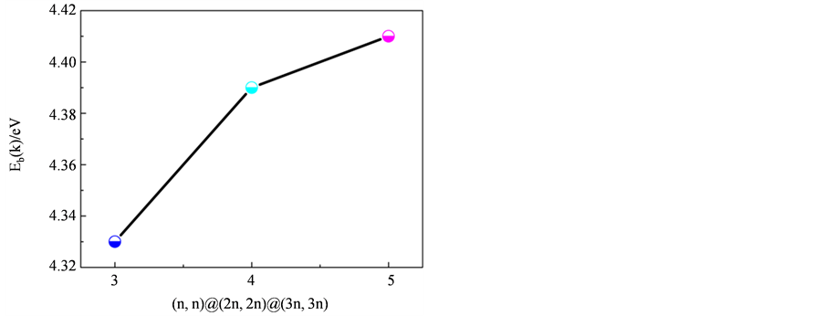
Figure 2. Average binding energy of (n, n)@(2n, 2n)@(3n, 3n) multi-walled silicon nanotubes
图2. (n, n)@(2n, 2n)@(3n, 3n)型多壁硅纳米管的平均结合能

Figure 3. Band structure of (n, n)@(2n, 2n)@(3n, 3n) multi- walled silicon nanotubes
图3. (n, n)@(2n, 2n)@(3n, 3n)型多壁硅纳米管的能带结构
由表1我们可以看出三壁硅纳米管的间接带隙逐渐减小,并且间接带隙与最小直接带隙的差 分别为0.138 eV,0.056 eV,0.005 eV;正如通常人们所认为的一样当
 小于0.01 eV时,可以将这个间接带隙半导体看作是准直接带隙半导体。如人们所知,间接带隙硅限制了光的反射,从而可以应用在光电领域。多壁硅纳米管揭示了硅材料可能存在直接带隙的情况。量子效应限制会使硅纳米材料的带隙增大,并且使能带结构从间接带隙变成准直接带隙。
3.3. 多壁硅纳米管的态密度
为进一步分析三壁硅纳米管的表面结构特性,本文研究两类纳米管的总态密度(TDOS)和分态密度(PDOS)。由图可知,多壁硅纳米管也是窄带隙半导体。图4中列出了(3, 3)@(6, 6)@(9, 9)和(4, 4)@(8, 8)@(12, 12)型硅纳米管在Fermi能级附近管壁的单个硅原子各轨道成分的DOS。每个DOS图内是该硅原子的s,p轨道的PDOS,其中取相对单位标定图谱的峰值。
从图4各DOS可以看出:
1) 管径较小的纳米管和管径较大的在费米能级附近的DOS分布无明显差异,如(3, 3)@(6, 6)@(9, 9)和(4, 4)@(8, 8)@(12, 12)型硅纳米管,所以管径对费米能级附近的能带成分影响不大;
2) 在费米附近的PDOS几乎为0,只有在−5 eV以下及5 eV以上才出现一些小峰,这表示费米能级附近的能带中基本不含S轨道成分。其原因是S轨道主要参与σ键,而各键的能量分布一般是:0 < π < π* < σ*,所以S轨道的PDOS就分布在较低的能量区间,于是EF附近的PDOS值就很小;
对几种多壁硅纳米管,通过DOS图和PDOS图分析其能带成分,指出管径对费米附近能带的成分无明显影响,而构成π键主要成分的P轨道的PDOS主要集中在费米能级附近。例如我们研究的[3,3]@[6,6]@[9,9]双壁硅纳米管的能带结构、总态密度和部分态密度。总的态密度能量分布在−5.4 eV至
Table 1. The results of the electronic structure of (n, n)@(2n, 2n)@(3n, 3n) are calculated by using the PBC method
表1. 用PBC方法对(n,n)@(2n,2n)@(3n,3n)型三壁硅纳米管电子结构的计算结果
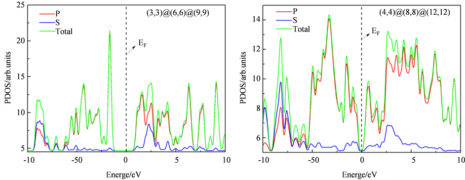
Figure 4. The TDOS and PDOS of (n, n)@(2n, 2n)@(3n, 3n) multi-walled silicon nanotubes
图4. (n, n)@(2n, 2n)@(3n, 3n)型多壁硅纳米管的TDOS和PDOS
0 eV范围内,形成了π电子能带;在2 eV~7 eV范围内,形成了σ电子能带。带隙约为1.2 eV,与[3,3]@[6,6]@[9,9]多壁壁管状团簇的能隙十分接近,说明了[3,3]@[6,6]@[9,9]多壁硅纳米管是窄带隙半导体。由部分态密度可以得到最高占据态和导带最低未占据态是由硅原子的P轨道贡献的。
由于费米能级附近的占据和空置状态能够决定材料的物理(如导电性)和化学性质(如亲核反应),因此希望上述结果能为使用硅纳米管的化学和物理特性提供指导。
4. 结论
扶手椅型多壁硅纳米管是间接窄带隙半导体,随着直径的增加,带隙逐渐减小,并且具有直接带隙的部分特征,可以看做是准直接带隙半导体。可以预见的是,硅的某些构型可能是直接带隙半导体。
致谢
感谢国家自然科学基金(批准号:11464044)的资助。
文章引用
刘登辉,唐宇超,姚程鹏,祝恒江. 扶手椅型多壁硅纳米管电子特性的密度泛函理论研究
Density Functional Theory Research of the Electronic Structure of Armchair Type Multi-Walled Silicon Nanotubes[J]. 材料科学, 2016, 06(03): 207-213. http://dx.doi.org/10.12677/MS.2016.63026
参考文献 (References)
- 1. Iijima S. (1991) Helical Microtubules of Graphitic Carbon. Nature, 354, 56-58. http://dx.doi.org/10.1038/354056a0
- 2. Jeong, S.Y., Kim, J.Y., Yang, H.D., et al. (2003) Synthesis o f Silicon Nanotubes on Porous Alumina Using Molecular Beamepiaxy. Advanced Materials, 15, 1172. http://dx.doi.org/10.1002/adma.200304898
- 3. Manzano-Ramirez, A., Moreno-Barcenas, A., Apatiga-Castro, M., et al. (2013) An Overview of Carbon Nanotubes: Synthesis, Purification and Characterization. Current Organic Chemistry, 17, 1858-1866. http://dx.doi.org/10.2174/13852728113179990087
- 4. Georgakilas, V., Perman, J.A., Tucek, J., et al. (2015) Broad Family of Carbon Nanoallotropes: Classification, Chemistry, and Applications of Fullerenes, Carbon Dots, Nanotubes, Graphene, Nano-Diamonds, and Combined Superstructures. Chemical Reviews, 115, 4744-4822. http://dx.doi.org/10.1021/cr500304f
- 5. Garcia-Borràs, M., Osuna, S., Luis, J.M., et al. (2014) The Role of Ar-omaticity in Determining the Molecular Structure and Reactivity of (Endohedralmetallo) Fullerenes. Chemical Society Reviews, 43, 5089-5105. http://dx.doi.org/10.1039/c4cs00040d
- 6. Pérez, E.M. and Martín, N. (2015) π-π Interactions in Carbon Nanostructures. Chemical Society Reviews, 44, 6425- 6433. http://dx.doi.org/10.1039/C5CS00578G
- 7. Daeneke, T., Carey, B.J., Chrimes, A.F., et al. (2015) Light Driven Growth of Silver Nanoplatelets on 2D MoS 2 Nanosheet Templates. Journal of Materials Chemistry C, 3, 4771-4778. http://dx.doi.org/10.1039/C5TC00288E
- 8. Biju, V. (2014) Chemical Modifications and Bioconjugate Reactions of Nanomaterials for Sensing, Imaging, Drug Delivery and Therapy. Chemical Society Reviews, 43, 744-764. http://dx.doi.org/10.1039/C3CS60273G
- 9. Cheng, L., Wang, C., Feng, L., et al. (2014) Functional Nanomaterials for Phototherapies of Cancer. Chemical Reviews, 114, 10869-10939. http://dx.doi.org/10.1021/cr400532z
- 10. Perreault, F., de Faria, A.F. and Elimelech, M. (2015) Environmental Applications of Graphene-Based Nanomaterials. Chemical Society Reviews, 44, 5861-5896. http://dx.doi.org/10.1039/C5CS00021A
- 11. Li, J. and Pandey, G.P. (2015) Advanced Physical Chemistry of Carbon Nanotubes. Annual Review of Physical Chemistry, 66, 635-651. http://dx.doi.org/10.1146/annurev-physchem-040214-121535
- 12. Salice, P., Sartorio, C., Burlini, A., et al. (2015) On the Trade-Off between Processability and Opto-Electronic Properties of Single Wall Carbon Nanotube Derivatives in Thin Film Heterojunctions. Journal of Materials Chemistry C, 3, 303-312. http://dx.doi.org/10.1039/C4TC01350F
- 13. Guo, L., Zheng, X., Liu, C., Zhou, W. and Zeng, Z. (2012) An Ab Initio Study of Cluster-Assembled Hydrogenated Silicon Nanotubes. Computational and Theoretical Chemistry, 982, 17-24.
- 14. Sha, J., Niu, J., Ma, X., et al. (2002) Silicon Nanotubes. Advanced Materials, 14, 1219-1221. http://dx.doi.org/10.1002/1521-4095(20020903)14:17<1219::AID-ADMA1219>3.0.CO;2-T
- 15. Fagan, S.B., Baierle, R.J., Mota, R., et al. (2000) Ab Initio Calculations for a Hypothetical Material: Silicon Nanotubes. Physical Review B, 61, 9994-9996. http://dx.doi.org/10.1103/PhysRevB.61.9994
- 16. Bai, J., Zeng, X.C., Tanaka, H. and Zeng, J.Y. (2004) Metallic Single-Walled Silicon Nanotubes. Proceedings of the National Academy of Sciences of the United States of America, 101, 2664-2668. http://dx.doi.org/10.1073/pnas.0308467101
- 17. Zhang, M., Kan, Y.H., Zhang, Q.J., Su, Z.M. and Wang, R.S. (2003) Why Silicon Nanotubes Stably Exist in Armchair Structure? Chemical Physics Letters, 379, 81-86. http://dx.doi.org/10.1016/j.cplett.2003.08.030
- 18. Saito, R., Fujita, M., Dresselhaus, G. and Dresselhaus, M.S. (1993) Electronic Structure and Growth Mechanism of Carbon Tubules. Materials Science and Engineering: B, 19, 185-191.
- 19. Zhen, W., Yokojima, S., Ng, M.-F., Hua, G. and He, G.Z. (2001) Optical Properties of Single-Wall 4 Å Carbon Nanotubes. Journal of the American Chemical Society, 123, 9830-9836. http://dx.doi.org/10.1021/ja0160445
- 20. Zhang, R.Q., Lee, H.L., Li, W.K. and Teo, B.K. (2005) Investigation of Possible Structures of Silicon Nanotubes via Density-Functional Tight-Binding Molecular Dynamics Simulations and Ab Initio Calculations. The Journal of Physical Chemistry B, 109, 8605-8612. http://dx.doi.org/10.1021/jp045682h
- 21. Barnard, A. and Russo, S.P. (2003) Structure and Energetics of Sin-gle-Walled Armchair and Zigzag Silicon Nanotubes. The Journal of Physical Chemistry B, 107, 7577-7581. http://dx.doi.org/10.1021/jp0347421
- 22. Singh, K.A., Briere, T.M., Kumar, V. and Kawazoe, Y. (2003) Mag-netism in Transition-Metal-Doped Silicon Nanotubes. Physical Review Letters, 91, Article ID: 146802. http://dx.doi.org/10.1103/PhysRevLett.91.146802
- 23. Tang, Y.H., Pei, L.Z., Chen, Y.W. and Guo, C.G. (2005) Self-Assembled Silicon Nanotubes under Supercritically Hydrothermal Condition. Physical Review Letters, 95, Article ID: 116102.
- 24. Frisch, M.J., et al. (2004) Gaussian 03, Revision E01. Gaussian, Inc., Wallingford CT.
- 25. Becke, A.D. (1993) Density-Functional Thermochemistry. III. The Role of Exact Exchange. The Journal of Chemical Physics, 98, 5648-5652. http://dx.doi.org/10.1063/1.464913
- 26. Lee, C., Yang, W. and Parr, R.G. (1988) Development of the Colle-Salvetti Correlation-Energy Formula into a Functional of the Electron density. Physical Review B, 37, 785-789. http://dx.doi.org/10.1103/PhysRevB.37.785
- 27. Hay, P.J. and Wadt, W.R. (1985) Ab Initio Effective Core Potentials for Molecular Calculations. Potentials for K to Au Including the Outermost Core Orbitals. The Journal of Chemical Physics, 82, 299-310. http://dx.doi.org/10.1063/1.448975
- 28. Hay, P.J. and Wadt, W.R. (1985) Ab Initio Effective Core Potentials for Molecular Calculations. Potentials for the Transition Metal Atoms Sc to Hg. The Journal of Chemical Physics, 82, 270-283. http://dx.doi.org/10.1063/1.448799
- 29. Wadt, W.R. and Hay, P.J. (1985) Ab Initio Effective Core Po-tentials for Molecular Calculations. Potentials for Main Group Elements Na to Bi. The Journal of Chemical Physics, 82, 284-298. http://dx.doi.org/10.1063/1.448800
- 30. Kudin, K.N. and Scuseria, G.E. (2000) Linear-Scaling Densi-ty-Functional Theory with Gaussian Orbitals and Periodic Boundary Conditions: Efficient Evaluation of Energy and Forces via the Fast Multipole Method. Physical Review B, 61, 16440-16453. http://dx.doi.org/10.1103/PhysRevB.61.16440
- 31. Erkoc, S. (2000) The Effect of PBC on the Simulation of Nanotubes. International Journal of Modern Physics C, 11, 547-551.
- 32. Pisani, C., Ed. (1996) Lecture Notes in Chemistry. Vol. 67, Springer-Verlag, Heidelberg.
- 33. Zhang, R.Q., Lee, S.T., Law, C.-K., Li, W.-K. and Teo, B.K. (2002) Silicon Nanotubes: Why Not? Chemical Physics Letters, 364, 251-258. http://dx.doi.org/10.1016/S0009-2614(02)01334-9
*通讯作者。