Material Sciences
Vol.
12
No.
05
(
2022
), Article ID:
51684
,
8
pages
10.12677/MS.2022.125054
磁控溅射法制备PMN-PZT/PZT异质薄膜的电性能
宛瑛泽,李克洪,孟令凤,张帅,杨志峰,邹赫麟*
大连理工大学,辽宁 大连
收稿日期:2022年4月21日;录用日期:2022年5月18日;发布日期:2022年5月25日
摘要
在Pt(111)/Ti/SiO2/Si(100)基底上覆盖Pb1.2(Zr0.40, Ti0.60)O3种子层,使用磁控溅射法在种子层上交替沉积0.3Pb(Mg1/3Nb2/3)O3-0.7Pb(Zr0.52Ti0.48)O3和Pb(Zr0.52Ti0.48)O3制备多层异质结构薄膜。研究异质界面数量不变的基础上,0.3Pb(Mg1/3Nb2/3)O3-0.7Pb(Zr0.52Ti0.48)O3和Pb(Zr0.52Ti0.48)O3厚度比变化对PZT性能的影响。通过XRD测得所有薄膜具备单一的钙钛矿相和(111)择优取向。使用扫描电子显微镜(SEM)观察到多层薄膜呈现致密的没有明显缺陷的钙钛矿结构。研究发现,在PMN-PZT和PZT的厚度比为2:1的条件下介电性能达到最佳,在频率为1 kHz时测得εr = 1237.9,tanδ = 0.048。使用标准铁电测试系统测得PMN-PZT和PZT的厚度比为的样品呈现饱和的P-E滞后曲线。此外,测得在电场下,PMN-PZT和PZT的厚度比为2:1的多层异质薄膜具有最小的漏电流密度为J = 5.5 × 10⁻⁸ A/cm2。
关键词
磁控溅射,多层PZT薄膜,厚度比,微观结构,电性能

Electrical Properties of PMN-PZT/PZT Heterostructure Films Prepared by Magnetron Sputtering
Yingze Wan, Kehong Li, Lingfeng Meng, Shuai Zhang, Zhifeng Yang, Helin Zou*
Dalian University of technology, Dalian Liaoning
Received: Apr. 21st, 2022; accepted: May 18th, 2022; published: May 25th, 2022

ABSTRACT
Pb1.2(Zr0.40, Ti0.60)O3 was covered on Pt(111)/Ti/SiO2/Si(100) substrate seed layer. Multilayer heterostructure films were prepared by alternately depositing 0.3Pb(Mg1/3Nb2/3)O3-0.7Pb(Zr0.52Ti0.48)O3 and Pb(Zr0.52Ti0.48)O3 on the seed layer by magnetron sputtering. The effects of the thickness ratio of 0.3Pb(Mg1/3Nb2/3)O3-0.7Pb(Zr0.52Ti0.48)O3 and Pb(Zr0.52Ti0.48)O3 on the properties of PZT were studied. All films have a single perovskite phase and (111) preferred orientation measured by XRD. Scanning electron microscopy (SEM) showed that the multilayer films showed a dense perovskite structure without obvious defects. It is found that the dielectric properties reach the best when the thickness ratio of PMN-PZT to PZT is 2:1, which is measured at the frequency of 1 kHz εr = 1237.9, tanδ = 0.048. The sample measured by standard ferroelectric test system shows a saturated P-E hysteresis curve of 2:1. In addition, it is measured that the multilayer heterostructure film with thickness ratio of 2:1 has the minimum leakage current density of J = 5.5 × 10⁻⁸ A/cm2.
Keywords:Magnetron Sputtering, Multilayer PZT Film, Thickness Ratio, Microstructure, Electrical Properties

Copyright © 2022 by author(s) and Hans Publishers Inc.
This work is licensed under the Creative Commons Attribution International License (CC BY 4.0).
http://creativecommons.org/licenses/by/4.0/


1. 介绍
锆钛酸铅(PZT)薄膜因铁电、介电以及压电特性优异,广泛应用于铁电存储器、可穿戴设备等多领域的研究当中 [1] [2]。目前PZT薄膜的制备常用金属有机化学气相沉积(MOCVD)法、溅射法、脉冲激光法(MOCVD)、溶胶凝胶法(Sol-Gel)等 [3] - [14]。其中,由于成型速度高、结晶良好,RF磁控溅射被广泛应用。
众多学者对于可能影响薄膜性能的因素 [15] [16] [17] 进行研究发现,掺杂 [7]、制备缓冲层以及制备多层薄膜等方法均能改善PZT薄膜的性能。组分不同的薄膜通过交替沉积的方法生成多层异质薄膜结构也越来越受到关注 [18] - [23]。Wang F等人发现掺杂浓度为0.1%的Ce离子的PZT薄膜具有优异的电性能。在0.1 kHz时,εr和tanδ分别为1326.9和0.063,2Pr为13.58 μC/cm2,比未掺杂Ce离子的样品提高42.4%。Wu J等人利用磁控溅射法在Pt上先后沉积了PbO缓冲层和PZT薄膜,制备出较高(100)择优取向的薄膜,电性能明显提高。Huiting S等人制备了PMN-PT/PZT多层异质结构薄膜,εr和tanδ分别为1959和0.0152。在400 kV/cm电场强度下,漏电流密度为9 × 10-8 A/cm2。表现出优异的介电和铁电性能。
本次工作中,先在Pt/Ti/SiO2/Si衬底上利用溶胶凝胶法制备了Pb1.2(Zr0.40, Ti0.60)O3种子层,然后在其采用原位溅射法沉积0.3Pb(Mg1/3Nb2/3)O3-0.7Pb(Zr0.52Ti0.48)O3/Pb(Zr0.52Ti0.48)O3(PMN-PZT/PZT)异质薄膜,具体参数如表1所列。沉积步骤如下:将PZT、PMN-PZT靶材装在腔室内相应位置,依次交替沉积,控制每层厚度比分别为1:2、1:3、3:1、2:1,形成异质界面数量为5,厚度约700 nm的多层异质结构薄膜,制备PZT和PMN-PZT薄膜作为对照组,异质结构薄膜示意图如图1所示。
2. 实验步骤
首先,制备PZT前驱体溶液,然后用滴管吸取前驱体溶液滴到吸附在托盘上的底电极上,利用旋涂法,低速600 r/min,12 s;高速2800 r/min,30 s,制得PZT湿膜,然后将其放置在150℃的干燥箱中保温5 min。然后放入常规马弗炉中5 min (去水分);450℃,5 min (热分解有机物);600℃,10 min (退火结晶)。重复上述步骤重得到缓冲层。
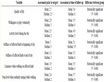
Table 1. Magnetron sputtering parameters
表1. 磁控溅射参数

Figure 1. Schematic diagram of PMN-PZT/PZT heterostructure film
图1. PMN-PZT/PZT异质结构薄膜示意图
然后,使用磁控溅射法采用原位溅射工艺沉积0.3Pb(Mg1/3Nb2/3)O3-0.7Pb(Zr0.52Ti0.48)O3/Pb(Zr0.52Ti0.48)O3(PMN-PZT/PZT)异质结构薄膜。对基片进行烘干和去水分。选定PZT和PMN-PZT两种靶材放置在强室内相应位置,将制备好的基底装入样品台,待腔室内真空度达到5.0 × 10−5 Pa后,通入氧氩混合气体,利用节流阀稳定气压;射频电源功率设置为150 W,开启射频匹配器,开始交替溅射多层异质薄膜,溅射时Ar的气体流量为90 sccm,腔室气压为2 Pa,样品台和靶材间的距离保持100 mm。先沉积PZT,再沉积PMN-PZT,交替沉积异质薄膜。表1列举了PZT薄膜的制备参数。
本文选用X射线衍射仪(D8 Bruker, Cu-Kα radiation, Bruker, Germany)布拉格角范围20˚ ≤ 2θ ≤ 60˚内,分析多层异质薄膜的晶体结构和结晶取向。薄膜微观形貌的表征选用扫描电子显微镜(SU8220, Hitachi, Japan)进行表征。使用阻抗分析仪(4294A, Agilent Technologies, US)测量PZT薄膜的介电性能,频率函数在0.1到100 KHz变化。多层异质薄膜的铁电性能使用标准铁电测试系统(Radiant Technologies)测量。
3. 结果和讨论
图2为PMN-PZT/PZT异质薄膜以及单一组分的PZT和PMN-PZT薄膜的XRD图谱。由图可知,纯PMN-PZT薄膜、PMN-PZT和PZT的厚度比分别为1:2、1:3、3:1和2:1型PMN-PZT/PZT异质薄膜均表现为高(111)择优取向的纯钙钛矿相。薄膜的择优取向程度可用以下公式定量表达 [24]:
(1)
公式中的 和 分别表示(100)和(111)峰的衍射强度。当PMN-PZT与PZT的厚度比小于2:1时,异质薄膜的(111)择优取向度较高是由于Mg、Nb含量能够影响薄膜的晶向结构。如最低表面能理论所述 [25],掺Mg、Nb能够促进PZT薄膜优先沿着(111)晶面成长,同时抑制其他取向的形核与生长。但随着PMN-PZT与PZT的厚度比到达3:1,过量的Mg、Nb无法全部进入PZT薄膜的晶格之中,在边界处产生聚集,PZT薄膜沿着(111)取向的形核生长受到抑制,导致异质薄膜的(111)择优取向度减小。此外,异质成核也会促进PZT薄膜沿择优取向生长。
![]()
Figure 2. XRD pattern of PMN-PZT/PZT heterogeneous films
图2. PMN-PZT/PZT异质薄膜的XRD图谱
图3为使用FE-SEM测得样品的截面形貌。单一组分的PZT、PMN-PZT以及PMN-PZT和PZT厚度比为2:1和3:1时的异质薄膜截面微观结构如图3所示,缓冲层和其上生长的薄膜之间有着微弱的界面,薄膜均为钙钛矿结构且柱状结构致密。厚度效应可能会降低钙钛矿结构的结晶驱动力 [26],进而导致纯PZT薄膜的柱状结构随着薄膜厚度的增加而逐渐模糊(图3(a)所示)。PMN-PZT相较于纯PZT柱状结构相对模糊,致密性较差,晶粒较小且表面较为粗糙,因为离子的替代会对晶粒形核生长产生抑制。由图可看出,PMN-PZT和PZT厚度比为2:1时,异质薄膜晶粒生长良好,晶界清晰,薄膜柱状结构致密性最好。研究结果表明,PMN-PZT和PZT厚度比变化对PZT薄膜的界面形貌有显著影响,PMN-PZT和PZT的厚度比(小于等于2:1)是多层异质结构薄膜表面均匀,柱状结构更为致密,而厚度比较大时,由于Mg、Nb离子在晶界处发生聚集,影响晶粒长大,导致PZT薄膜柱状结构致密程度下降。
![]() (a) PZT
(a) PZT
![]() (b) PMN-PZT
(b) PMN-PZT
![]() (c) 2:1
(c) 2:1
![]() (d) 3:1
(d) 3:1
Figure 3. Interface diagram of all samples: (a) PZT; (b) PMN-PZT; (c) 2:1; (d) 3:1
图3. 所有样品的界面图:(a) PZT;(b) PMN-PZT;(c) 2:1;(d) 3:1
图4(a) 为单一组分的PZT、PMN-PZT薄膜以及PMN-PZT/PZT异质薄膜的P-E回线。图中可以看出,磁滞回线均饱和,如图4(b)所示,PMN-PZT和PZT的厚度比为2:1的样品剩余极化Pr = 21 μC/cm2和矫顽场强Ec = 90 kV/cm,二者均较大。这可能是由于多层异质结构和内应力的改变。此外PMN-PZT和PZT的厚度比为2:1的样品(111)择优取向度较大,因而相对于其他样品而言,Pr有所提高。PMN-PZT和PZT的厚度比为2:1的样品具有最佳的铁电性能。PZT薄膜的铁电性能在受结晶取向影响的同时,还与薄膜组分有关,因此由于厚度变化造成的离子浓度的改变使得其他样品的铁电性能明显不如PMN-PZT和PZT的厚度比为2:1的样品。层间耦合效应增强能够促进畴壁运动,这也是铁电性能得到提升的原因之一。
![]() (a)
(a) ![]() (b)
(b)
Figure 4. Ferroelectric characteristics of thin film: (a) P-E loop; (b) 2Pr and 2Ec values
图4. 薄膜铁电特性:(a) P-E回线;(b) 2Pr和2Ec值
图5为制备的异质结构薄膜在0.1~100 kHz频率范围内的介电常数和损耗因子变化趋势。从图中可以看出,随着频率的增大多层异质结构薄膜的εr减小,tanδ先减小后增大。PMN-PZT和PZT的厚度比为2:1的样品的介电常数最大,在1 kHz时,εr = 1237.9,相比于其他厚度比的异质结构薄膜介电常数εr较大介电损耗tanδ较小。有研究发现极化方向与薄膜的择优生长取向有着一定的关联所以厚度比为2:1的样品介电性能的提高可能是由于其高(111)择优取向。由于厚度效应和界面耦合效应的作用,交替沉积的薄膜的电性能会有相应的提高,这也是PMN-PZT和PZT的厚度比为2:1的样品电性能提高的原因。偶极子损耗、自由电荷等也可能是产生这一影响的原因 [27]。
![]() (a)
(a)  (b)
(b)
Figure 5. Dielectric properties of thin film: (a) Relationship between dielectric constant and frequency; (b) Relationship between dielectric loss and frequency
图5. 薄膜介电特性:(a) 介电常数随频率变化关系;(b) 介电损耗随频率变化关系
异质结构薄膜的漏电流密度如图6所示。从图中可以看到,漏电流密度随着电场强度的增大而增大。多层薄膜的漏电流密度有所降低。其中,PMN-PZT样品具有最大的漏电流密度9.37 × 10⁻⁷ A/cm2。对于多层薄膜样品,随着薄膜交替溅射薄膜厚度的增加,漏电流密度逐渐减小。PMN-PZT和PZT的厚度比为2:1相较于PMN-PZT和PZT的厚度比为1:3 (2.67 × 10⁻⁷ A/cm2)和PMN-PZT和PZT的厚度比为1:2 (8.26 × 10⁻⁷ A/cm2)的漏电流密度低了接近一个数量级,仅为5.5 × 10−8 A/cm2。观察到的J-E特性与介电性能测试结果比较符合。

Figure 6. Leakage current density of all PZT films
图6. 所有PZT薄膜的漏电流密度
4. 结论
使用磁控溅射法成功的在Pb1.10(Zr0.52, Ti0.48)O3作为种子层,Pt(111)/Ti/SiO2/Si(100)基底上制备了由0.3Pb(Mg1/3Nb2/3)O3-0.7Pb(Zr0.52Ti0.48)O3和Pb(Zr0.52Ti0.48)O3组成的铁电多层薄膜。经XRD分析,多层薄膜的(111)择优取向度较高。SEM图显示薄膜有着致密均匀的柱状结构的钙钛矿相。PMN-PZT与PZT的厚度比为2:1的多层异质薄膜具有最佳的介电性能,εr = 1237.9和tanδ = 0.046。PMN-PZT和PZT的厚度比为2:1的多层异质薄膜相比其它薄膜具有更好的铁电性能,Pr = 21.3 μC/cm2,Ec = 88.1KV/cm。此外,PMN-PZT和PZT的厚度比为2:1的多层异质薄膜在电场作用下的漏电流密度最小,J = 5.5 × 10⁻⁸ A/cm2。
文章引用
宛瑛泽,李克洪,孟令凤,张 帅,杨志峰,邹赫麟. 磁控溅射法制备PMN-PZT/PZT异质薄膜的电性能
Electrical Properties of PMN-PZT/PZT Heterostructure Films Prepared by Magnetron Sputtering[J]. 材料科学, 2022, 12(05): 516-523. https://doi.org/10.12677/MS.2022.125054
参考文献
- 1. Haertling, G.H. (1999) Ferroelectric Ceramics: History and Technology. Journal of the American Ceramic Society, 82, 797-818. https://doi.org/10.1111/j.1151-2916.1999.tb01840.x
- 2. 孙慷, 张幅学. 压电学[M]. 北京: 国防工业出版社, 1984: 117-120.
- 3. Izyumskaya, N., Alivov, Y., Cho, S.J., Morkoç, H., Lee, H. and Kang, Y.-S. (2007) Processing, Structure, Properties, and Applications of PZT Thin Films. Critical Reviews in Solid State and Materials Sciences, 32, 111-202. https://doi.org/10.1080/10408430701707347
- 4. He, B. and Wang, Z. (2016) Enhancement of the Electrical Prop-erties in BaTiO3/PbZr0.52Ti0.48O3 Ferroelectric Superlattices. ACS Applied Materials & Interfaces, 8, 6736-6742. https://doi.org/10.1021/acsami.5b12098
- 5. Datta, A., Mukherjee, D., Witanachchi, S. and Mukherjee, P. (2014) Hierarchically Ordered Nano-Hetero Structured PZT Thin Films with Enhanced Ferroelectric Properties. Advanced Func-tional Materials, 24, 2638-2647. https://doi.org/10.1002/adfm.201303290
- 6. Vrejoiu, I., Zhu, Y., Rhun, G.L., Andreas Schubert, M., Hesse, D. and Alexe, M. (2007) Structure and Properties of Epitaxial Ferroelectric PbZr0.4Ti0.6O3/PbZr0.6Ti0.4O3 Superlattices Grown on SrTiO3 (001) by Pulsed Laser Deposition. Applied Physics Letters, 90, Article ID: 072909. https://doi.org/10.1063/1.2643259
- 7. 赵海波. 水热合成法制备PZT压电薄膜的研究[D]: [硕士学位论文]. 大连: 大连理工大学, 2006.
- 8. Ma, B., Liu, S., Tong, S., Narayanan, M. and (Balu) Balachandran, U. (2012) En-hanced Dielectric Properties of Pb0.92La0.08Zr0.52Ti0.48O3 Films with Compressive Stress. Journal of Applied Physics, 112, Article ID: 114117. https://doi.org/10.1063/1.4768926
- 9. Masruroh (2013) Influence of the Waveform and DC Offset on the Asym-metric Hysteresis Loop in Au/PZT/Pt/Al2O3/SiO2/Si Thin Films Prepared by MOCVD Method. Applied Mechanics and Materials, 467, 155-159. https://doi.org/10.4028/www.scientific.net/AMM.467.155
- 10. Kingon, A.I. and Srinivasan, S. (2005) Lead Zir-conate Titanate Thin Films Directly on Copper Electrodes for Ferroelectric, Dielectric and Piezoelectric Applications. Na-ture Materials, 4, 233-237. https://doi.org/10.1038/nmat1334
- 11. Kim, J., Yang, S.A., Choi, Y.C., Han, J.K., Jeong, K.O., Yun, Y.J., et al. (2008) Ferroelectricity in Highly Ordered Arrays of Ultra-Thin-Walled Pb(Zr,Ti)O3 Nanotubes Composed of Nanometer-Sized Perovskite Crystallites. Nano Letters, 8, 1813-1818. https://doi.org/10.1021/nl080240t
- 12. Higuchi, K., Miyazawa, K., Sakuma, T. and Suzuki, K. (1994) Microstruc-ture Characterization of Sol-Gel Derived PZT Films. Journal of Materials Science, 29, 436-441. https://doi.org/10.1007/BF01162503
- 13. Fujii, T., Hishinuma, Y., Mita, T. and Naono, T. (2010) Characterization of Nb-Doped Pb(Zr,Ti)O3 Films Deposited on Stainless Steel and Silicon Substrates by RF-Magnetron Sputtering for MEMS Applications. Sensors and Actuators A: Physical, 163, 220-225. https://doi.org/10.1016/j.sna.2010.08.019
- 14. Krupanidhi, S.B., Maffei, N., Sayer, M. and El-Assal, K. (2011) R.F. Magnetron Sputtering of Ferroelectric PZT Films. Ferroelectrics, 51, 93-98. https://doi.org/10.1080/00150198308009058
- 15. Han, H., Song, X., Zhong, J., Kotru, S., Padmini, P. and Pan-dey, R.K. (2004) Highly α-Axis-Oriented Nb-Doped Pb(TixZr1−x)O3 Thin Films Grown by Sol-gel Technique for Un-cooled Infrared Dectors. Applied Physics Letters, 85, 5310-5312. https://doi.org/10.1063/1.1825062
- 16. Wang, Z.J., Kokawa, H. and Maeda, R. (2005) In Situ Growth of Lead Zirconate Titanate Thin Films by Hybrid Process: Sol-gel Method and Pulsed-Laser Deposition. Acta Materialia, 53, 593-600. https://doi.org/10.1016/j.actamat.2004.10.012
- 17. Wang, Z.J., Kokawa, H., Takizawa, H., Ichiki, M. and Maeda, R. (2005) Low-Temperature Growth of High-Quality Lead Zirconate Titanate Thin Films by 28 GHz Microwave Irradia-tion. Applied Physics Letters, 86, Article ID: 212903. https://doi.org/10.1063/1.1935748
- 18. Kanda, K., Hirai, S., Fujita, T. and Maenaka, K. (2018) Piezoelectric MEMS with Multilayered Pb(Zr,Ti)O3 Thin Films for Energy Harvesting. Sensors and Actuators A: Physical, 281, 229-235. https://doi.org/10.1016/j.sna.2018.09.018
- 19. Bousquet, E., Dawber, M., Stucki, N., Lichtensteiger, C., Hermet, P., Gariglio, S., et al. (2008) Improper Ferroelectricity in Perovskite Oxide Artificial Superlattices. Nature, 452, 732-736. https://doi.org/10.1038/nature06817
- 20. Xu, H., Feng, M., Liu, M., Sun, X., Wang, L., Jiang, L., et al. (2018) Strain-Mediated Converse Magnetoelectric Coupling in La0.7Sr0.3MnO3/Pb(Mg1/3Nb2/3)O3-PbTiO3 Multiferroic Hetero-structures. Crystal Growth & Design, 18, 5934-5939. https://doi.org/10.1021/acs.cgd.8b00702
- 21. Tang, Y., Zhu, B., Wang, F., Sun, D., Hu, Z., Qin, X., et al. (2016) Dielectric and Ferroelectric Properties of (111) Preferred Oriented PbZr0.53Ti0.47O3/Pb(Mg1/3Nb2/3)0.62Ti0.38O3/PbZr0.53Ti0.47O3 Trilayered Films. Applied Surface Science, 371, 160-163. https://doi.org/10.1016/j.apsusc.2016.02.213
- 22. Zhang, T., Zhang S-Y, Wasa, K., Zhang, H., Chen, Z.-J., Shui, X.-J. et al. (2011) Effects of Pb(Mn,Nb)O3 Doping on the Properties of PZT-Based Films Deposited on Silicon Sub-strates. Physica Status Solidi (A), 208, 2460-2466. https://doi.org/10.1002/pssa.201026561
- 23. Lian, J., Ponchel, F., Tiercelin, N., Han, L., Chen, Y., Rémiens, D., et al. (2018) Influence of the Magnetic State on the Voltage-Controlled Magnetoelectric Effect in A Multiferroic Artificial Heterostructure YIG/PMN-PZT. Journal of Applied Physics, 124, Article ID: 064101. https://doi.org/10.1063/1.5037057
- 24. 许立宁. 基于MEMS技术的压电微喷的研制[D]: [博士学位论文]. 北京: 中国科学院研究生院(电子学研究所), 2005.
- 25. Yang, F., Fei, W.D. and Sun, Q. (2009) Highly (100)-Textured Pb(Zr0.52Ti0.48)O3 Film Derived From A Modified Sol–gel Technique Using Inorganic Zirconium Precursor. Journal of Materials Processing Technology, 209, 220-224. https://doi.org/10.1016/j.jmatprotec.2008.01.042
- 26. Es-Souni, M., Abed, M., Solterbeck, C.H. and Piorra, A (2002) Crystallization Kinetics and Dielectric Properties of Solution Deposited, La Doped PZT Thin Films. Materials Science and Engineering B-Solid State Materials for Advanced Technology, 94, 229-236. https://doi.org/10.1016/S0921-5107(02)00099-5
- 27. Kanno, I. (2018) Piezoelectric MEMS: Ferroelectric Thin Films for MEMS Applications. Japanese Journal of Applied Physics, 57, Article ID: 040101. https://doi.org/10.7567/JJAP.57.040101
NOTES
*通讯作者。