 Material Sciences 材料科学, 2013, 3, 116-120 http://dx.doi.org/10.12677/ms.2013.33022 Published Online May 2013 (http://www.hanspub.org/journal/ms.html) Structural and Optical Properties of ZnO Thin Films Grown on MgO(111) Substrates by Molecular Beam Epitaxy Damin Du, Huiqiong Wang*, Hua Zhou, Yaping Li, Wei Huang, Jianfang Xu, Jiafa Cai, Linzhe Cui, Chunmiao Zhang, Xiaohang Chen, Huahan Zhan, Junyong Kang Key Laboratory of Semiconductors and Applications of Fujian Province, Department of Physics, Xiamen University, Xiamen Email: *hqwang@xmu.edu.c Received: Apr. 24th, 2013; revised: Apr. 26th, 2013; accepted: May 7th, 2013 Copyright © 2013 Damin Du et al. This is an open access article distributed under the Creative Commons Attribution License, which permits unre- stricted use, distribution, and reproduction in any medium, provided the original work is properly cited. Abstract: The growth of high quality ZnO films is highly desirable due to the promising applications of ZnO in opto- electronics. In this paper, ZnO films were grown on the MgO(111) substrates via the growth technique of molecular- beam epitaxy and their structural and optoelectronic properties were characterized. In particular, the influence of growth condition on the film qualify was investigated. The results show that, inducing a low temperature ZnO buffer layer be- fore the high temperature growth of ZnO films will help to improve the film quality. In situ reflection high-energy elec- tron diffraction (RHEED) and ex situ X-ray Diffraction (XRD) measurements indicate that the ZnO film and the MgO substrate follow the epitaxial relationship: ZnO[1-210]//MgO[1-10] and ZnO[1-100]//MgO[11-2]. Transmission Spectra show the characteristic optical bandgap of ZnO. Keywords: MBE; RHEED; XL; Buffer; Dislocation Density MgO(111)上ZnO薄膜的外延生长及其结构和光学特性 杜达敏,王惠琼*,周 华,李亚平,黄 巍,徐建芳,蔡加法,崔琳哲,张纯淼,陈晓航,詹华瀚,康俊勇 厦门大学物理系,福建省半导体材料及应用重点实验室,厦门 Email: *hqwang@xmu.edu.cn 收稿日期:2013 年4月24 日;修回日期:2013年4月26 日;录用日期:2013 年5月7日 摘 要:由于ZnO 在光电器件的应用前景,其高质量薄膜的制备是研究热点之一。本文通过分子束外延生长法 在MgO(111)单晶衬底上生长 ZnO 薄膜,表征了其结构和特性,探讨了不同生长条件对薄膜质量的影响。结果 表明,先低温生长 ZnO缓冲层,再高温生长 ZnO薄膜,有望提高 ZnO 薄膜的质量。原位反射高能电子束衍射 (RHEED)和异位的 X射线衍射(XRD)分别测量出薄膜的面内结构和沿[0001]的单晶域高取向结构,并确定薄膜和 衬底的外延关系为ZnO[1-210]//MgO[1-10]和ZnO[1-100]//MgO[11-2]。透射谱显示了 ZnO 的特征光学带隙。 关键词:分子束外延;反射高能电子衍射;透射谱;缓冲层;位错密度 1. 引言 ZnO 作为第三代宽禁带半导体材料,因其激子束 缚能(室温下为60 meV)远高于 GaN,并具有更高的化 学稳定性和低成本等优势,从而在紫外发光二极管和 激光器等方面有着广泛的应用前景[1-5]。ZnO 在室温下 呈六方的纤锌矿结构,可通过在具有六方结构的 ZnO, GaN 和蓝宝石等衬底上外延获得[6]。其中蓝宝石因成 本相对更低而成为最常用的外延衬底。然而蓝宝石和 ZnO 薄膜之间有较大的晶格失配度(18%),常常导致 *通讯作者。 Copyright © 2013 Hanspub 116  MgO(111)上ZnO 薄膜的外延生长及其结构和光学特性 所生长的 ZnO 薄膜呈30˚旋转,薄膜质量较差,其表 面粗糙度也较大。引入低温MgO 或者同质低温 ZnO 缓冲层可以极大地改善外延ZnO 薄膜的晶体质量,有 效地减低位错密度[7-9]。但是在蓝宝石上生长ZnO 时, 在引入 MgO 缓冲层的同时,也存在着因 MgO 厚度变 化而引起的从纤锌矿向岩盐矿转化的相变问题[10],缓 冲层中存在的ZnMgO 团簇也可能导致可见光的发射 [11]。本文利用分子束外延技术(MBE) ,直接在单晶 MgO(111)衬底上外延生长 ZnO 薄膜,研究生长条件 对ZnO 薄膜质量的影响,获得单域C轴取向的 ZnO 薄膜,结果表明加入低温 ZnO 缓冲层的薄膜质量相对 较好。另一方面,以半导体为基础的有源器件和以功 能立方钙钛矿型氧化物为基础的无源器件是现代微 电子器件的需求之一[12-15]。研究 ZnO 在立方的 MgO 衬底上的生长机制,也有望为 ZnO 和更复杂的立方钙 钛矿的结合提供初步的制备指南。 2. 实验方法 生长实验在配备有原位的RHEED、扫描隧道显 微镜(STM)等表面探测技术的 OMICON 超高真空 MBE 系统中进行。在放入MBE 生长腔之前,单晶 MgO(111)衬底用丙酮和酒精在室温下交替超声清洗 三遍,每遍 5分钟。在放入生长腔之后,MgO(111) 衬底先在温度为350℃,氧偏压为 6.5 × 10⁻⁵ mbar,射 频功率为250 W的条件下退火一小时。生长时,先在 衬底温度为 380℃,氧偏压为6.5 × 10⁻⁵ mbar,射频功 率为 250 W的条件下低温生长 10 分钟的缓冲层;再 在525℃下高温退火 45 分钟(氧偏压仍为 6.5 × 10⁻⁵ mba r ,射频功率仍为 250 W);最后在更高的衬底温度 550℃,氧偏压 5 × 10⁻⁵ mbar和功率 250 W的高温条 件下生长一小时。为了作比较,另一组生长实验没有 引入缓冲层,而是改变衬底温度,分别在200℃、300 ℃和 350℃的条件下直接生长ZnO 薄膜。氧偏压和射 频功率和引入缓冲层时的高温生长条件一样。实验中 Zn 源的纯度为 99.9999%,蒸发源炉的温度保持在 360 ℃。通过反射高能电子衍射(RHEED)、X射线衍射 (XRD)等表征了薄膜和衬底的外延关系,并通过 XRD 的半高宽以及原子力显微镜(AFM)所测得的表面粗糙 度比较了衬底温度以及加入低温 ZnO 缓冲层等生长 条件对薄膜质量的影响。光学特性通过透射谱(XL)进 行表征。 3. 实验结果和讨论 图1为MgO(111)衬底上外延ZnO 时先引入低温 缓冲层再高温生长的原位 RHEED 图的演变情况。退 火后的 MgO(111)表面为(1 × 1)结构,显示出良好的表 面平整,如图 1(a)中的 RHEED 所示。其中电子束入 射方向分别沿着[1-10]和[11-2]晶轴。当低温ZnO 缓冲 层生长 30 秒时,开始出现 ZnO 的衍射图样,衍射点 的间距比衬底 MgO 的小 2%,这是由于 C轴方向 ZnO 受到压应力的缘故。随着生长的进行,ZnO 的衍射点 逐渐变得清晰,10 分钟的低温生长后,衍射斑点的间 距比衬底小 8.8%,并在后续的 525℃高温退火 45分 (a) (b) (c) (d) Figure 1. Evolution of RHEED patterns during the ZnO film growth on MgO(111): (a) MgO(111) surface after oxygen plasma treatment; (b) ZnO buffer layer at 380˚C for 10 mins; (c) After the annealing of the buffer layer at 525˚C for 45 mins; (d) After the growth of thick ZnO films at 550˚C for 60 mins. The two dashed boxes corresponded to the two reciprocal lattices (a1 *, c1 *) and (a2 *, c2 *) in (c), respectively 图1. 在MgO(111)上生长 ZnO 的RHEED 衍射图样:(a) 退火处 理后 MgO(111);(b) 380℃生长 10 mins 的ZnO 缓冲层;(c) 缓冲 层在 525℃退火 45 分钟;(d) 高温 550℃生长 60 分钟。其中(c) 图 * * 中虚线矩形框(a1, c1 *)和(a2, c2 *)分别代表 ZnO 的两套倒易晶格 Copyright © 2013 Hanspub 117 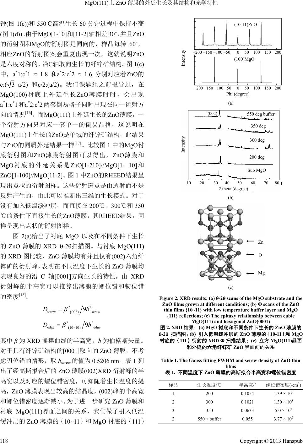 MgO(111)上ZnO 薄膜的外延生长及其结构和光学特性 钟 明 (图1(c))和550℃高温生长 60分钟过程中保持不变 (图1(d))。由于MgO[1-10 ]和[11-2]轴相差 30˚,并且ZnO 的衍射图和MgO的衍射图是同向的,样品每转 60˚, 相应ZnO的衍射图案会重复出现一次,这就说 ZnO 是六度对称的,沿C轴取向生长的纤锌矿结构。图 1(c) 中,a*1:c*1 ≈ 1.8和a*2:c*2 ≈ 1.6分别对应着ZnO的 c:( 3 a/2) 和c/2:(a/2) 。我们课题组之前报导过,在 Mg (100)衬底上外延生长ZnO 薄膜时时,会出现 a*1:c*1和a*2:c*2两套倒易格子同时出现在同一衍射方 向的情况[16]。而MgO(111)上外延生长的ZnO薄膜,一 个衍射方向只对应一套单一的倒易晶格,这说明在 MgO(111)上生长的ZnO是单域的纤锌矿结构,此结果 与ZnO的同质外延结果一样[17]。比较图1中的MgO衬 底衍射图和ZnO薄膜衍射图可以得出,ZnO薄膜和 MgO 衬底的外延关系是ZnO[1-210]//MgO[1- 10]和 ZnO[1-100]//MgO[11-2]。图 1中ZnO的RHEED结果呈 现出点状的衍射图样。这些衍射斑点是由透射而不是 反射产生的,由此可以推断出三维的生长模式。对于 没有加入低温缓冲层,而直接在 200℃、300℃和 350 ℃的条件下直接生长的ZnO薄膜,其RH EED 结果,同 样呈现出点状的衍射图样。 图2(a)给出了衬底MgO O 以及在不同条件下生长 的ZnO -薄膜的 XRD 2扫描图。与衬底 MgO(111) 的XRD 图比较,ZnO 薄膜均有并且仅有(002)六角纤 锌矿的衍射峰,表明在不同温度下生长的ZnO 薄膜均 表现良好的沿 C轴[0001]方向生长的特性。由XRD 衍射峰的半高宽可以推算出薄膜的螺位错和韧位错 的密度[18]: 22 screw screw 002 9Db 22 edge edge 10 109Db 其中 β为XRD 摇摆曲线的半高宽,b为伯格斯矢量。 对于具有纤锌矿结构的[0001]取向的ZnO 薄膜,不考 虑刃位错的情形,取 bscrew 的值为 0.5206 nm。表 1列 出了经高斯拟合后的 ZnO 薄膜(002)XRD 衍射峰的半 高宽以及对应的螺位错密度,可知随着生长温度的提 高,ZnO 薄膜表现出较高的结晶度,(002)峰的半高宽 和螺位错密度逐渐减小。为了进一步研究 ZnO 薄膜和 衬底 MgO(111)界面之间的关系,我们做了引入低温 缓冲层的ZnO 薄膜的{10~11}和 MgO 衬底的{111} (10-11)ZnO −200 −150 −100 −50 0 50 100 150 200 (100)MgO −200 −150 −100 −50 0 50 100 150 200 Phi (degree) Intensity (a) ( 002 ) 10 20 30 40 50 60 70 80 2 theta (degree) Intensity 550 deg buffer 350 deg 300 deg 200 deg Sub MgO (b) Zn O Mg (c) Figure 2. XRD results: (a) -2 scans of the MgO substrate and the 图 Table 1. The GauZnO thin ) ZnO films grown at different conditions; (b) Φ scans of the ZnO thin films {10~11} with low temperature buffer layer and MgO {111} reflections; (c) The epitaxy relationship between cubic MgO(111) and hexagonal ZnO(0001) 2. XRD 结果:(a) MgO 衬底和不同条件下生长的 ZnO 薄膜的 (b) 缓冲层的 ZnO 薄膜的{1-2 扫描图; 引入低温0-11}和 MgO 衬底的{111}衍射的 XRD Φ扫描结果;(c) 立方 MgO(111)晶面 和外延的六角纤锌矿 ZnO 界面间的关系 ss fitting FWHM and screw density of films 表1. 不同温度下 ZnO 薄膜的高斯拟合半高宽和螺位错密度 样品 生长温度/℃ 半高宽/˚ 螺位错密度(/cm2 1 200 0.1054 1.39 × 10⁸ 2 300 0.1021 1.30 × 10⁸ 3 350 0.0633 5.0 × 10⁷ 2 550fer + buf0.055 3.77 × 10⁷ Copyright © 2013 Hanspub 118 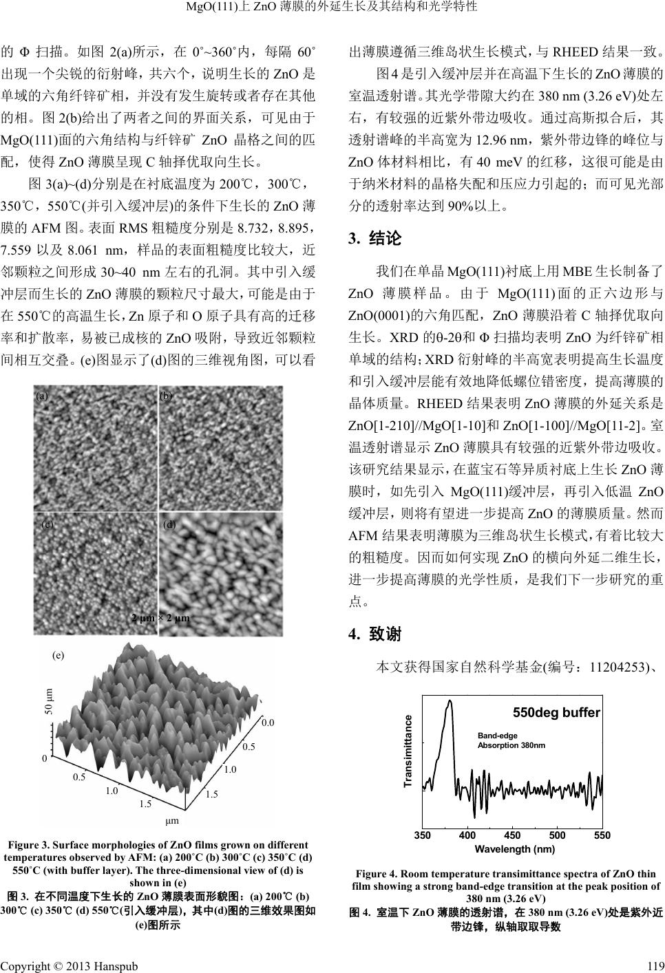 MgO(111)上ZnO 薄膜的外延生长及其结构和光学特性 的Φ如示,在 360˚内˚ 0℃, 350℃ 扫描。图 2(a)所0˚~,每隔60 出现一个尖锐的衍射峰,共六个,说明生长的 ZnO 是 单域的六角纤锌矿相,并没有发生旋转或者存在其他 的相。图 2(b)给出了两者之间的界面关系,可见由于 MgO(111)面的六角结构与纤锌矿 ZnO 晶格之间的匹 配,使得ZnO 薄膜呈现 C轴择优取向生长。 图3(a)~(d)分别是在衬底温度为200℃,30 ,550℃(并引入缓冲层)的条件下生长的 ZnO 薄 膜的 AFM图。表面 RMS 粗糙度分别是8.732,8.895, 7.559以及 8.061 nm,样品的表面粗糙度比较大,近 邻颗粒之间形成 30~40 nm左右的孔洞。其中引入缓 冲层而生长的ZnO 薄膜的颗粒尺寸最大,可能是由于 在550℃的高温生长,Zn 原子和 O原子具有高的迁移 率和扩散率,易被已成核的ZnO 吸附,导致近邻颗粒 间相互交叠。(e)图显示了(d)图的三维视角图,可以看 (a) (c) (d) (b) 2 μm × 2 μm (e) 0 0.5 1.0 1.5 1.0 1.5 0.5 0.0 μm 50 μm Figure 3. Surface morphologies of ZnO films grown on different 图 300 室温 单晶 MgO(111)衬底上用 MBE 生长制备了 ZnO 谢 得国家自然科学基金(编号:11204253)、 temperatures observed by AFM: (a) 200˚C (b) 300˚C (c) 350˚C (d) 550˚C (with buffer layer). The three-dimensional view of (d) is shown in (e) 3. 在不同温度下生长的 ZnO 薄膜表面形貌图:(a) 200℃ (b) 层),℃ (c) 350℃ (d) 550℃(引入缓冲 其 中 (d)图的三维效果图如 (e)图所示 出薄膜遵循三维岛状生长模式,与RHEED 结果一致。 图4是引入缓冲层并在高温下生长的 ZnO 薄膜的 透射谱。其光学带隙大约在 380 nm (3.26 eV)处左 右,有较强的近紫外带边吸收。通过高斯拟合后,其 透射谱峰的半高宽为 12.96 nm,紫外带边锋的峰位与 ZnO 体材料相比,有 40 meV的红移,这很可能是由 于纳米材料的晶格失配和压应力引起的;而可见光部 分的透射率达到90%以上。 3. 结论 我们在 薄膜样品。由于 MgO(111) 面的正六边形与 ZnO(0001)的六角匹配,ZnO 薄膜沿着C轴择优取向 生长。XRD 的-2和Φ扫描均表明ZnO 为纤锌矿相 单域的结构;XRD 衍射峰的半高宽表明提高生长温度 和引入缓冲层能有效地降低螺位错密度,提高薄膜的 晶体质量。RHEED 结果表明 ZnO 薄膜的外延关系是 ZnO[1-210]//MgO[1-10]和ZnO[1-100]//MgO[11-2]。室 温透射谱显示ZnO 薄膜具有较强的近紫外带边吸收。 该研究结果显示,在蓝宝石等异质衬底上生长ZnO 薄 膜时,如先引入 MgO(111) 缓冲层,再引入低温 ZnO 缓冲层,则将有望进一步提高ZnO 的薄膜质量。然而 AFM结果表明薄膜为三维岛状生长模式,有着比较大 的粗糙度。因而如何实现ZnO 的横向外延二维生长, 进一步提高薄膜的光学性质,是我们下一步研究的重 点。 4. 致 本文获 350 400 450 500 55 0 Band-edge Absorption 380nm 550deg buffer Waveleng th (n m ) Transimittance Figure 4. Room temperature transimittance spectra onO thin film showing a strong band-edge transition at the peakosition of 带边 数 f Z p 380 nm (3.26 eV) 图4. 室温下 ZnO 薄膜的透射谱,在 380 nm (3.26 eV)处是紫外近 锋,纵轴取取导 Copyright © 2013 Hanspub 119 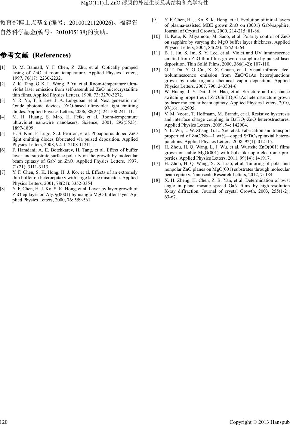 MgO(111)上ZnO 薄膜的外延生长及其结构和光学特性 Copyright © 2013 Hanspub 120 参考文献 (References) Zhu, et al. Optically pumped ature. Applied Physics Lette lution of initial layers ntrol of ZnO nd UV luminescence ed elec- Structure and resistance ofmann, M. Brandt, et al. Resistive hysteresis ansport ) films lar and f twist 教育部博士点基金(编号:20100121120026) 、福建省 自然科学基金(编号:2010J05138)的资助。 [1] D. M. Bannall, Y. F. Chen, Z. lasing of ZnO at room temperrs, t 1997, 70(17): 2230-2232. [2] Z. K. Tang, G. K. L. Wong, P. Yu, et al. Room-temperature ultra- violet laser emission from self-assembled ZnO microcrystalline thin films. Applied Physics Letters, 1998, 73: 3270-3272. [3] Y. R. Yu, T. S. Lee, J. A. Lubguban, et al. Next generation of Oxide photonic devices: ZnO-based ultraviolet light emitting diodes. Applied Physics Letters, 2006, 88(24): 241108-241111. [4] M. H. Huang, S. Mao, H. Feik, et al. Room-temperature ultraviolet nanowire nanolasers. Science, 2001, 292(5523): 1897-1899. [5] H. S. Kim, F. Lugo, S. J. Pearton, et al. Phoaphorus doped ZnO light emitting diodes fabricated via pulsed deposition. Applied Physics Letters, 2008, 92: 112108-112111. [6] F. Hamdani, A. E. Botchkarev, H. Tang, et al. Effect of buffer layer and substrate surface polarity on the growth by molecular beam epitaxy of GaN on ZnO. Applied Physics Letters, 1997, 71(21): 3111-3113. [7] Y. F. Chen, S. K. Hong, H. J. Ko, et al. Effects of an extremely thin buffer on heteroepitaxy with large lattice mismatch. Applied Physics Letters, 2001, 78(21): 3352-3354. [8] Y. F. Chen, H. J. Ko, S. K. Hong, et al. Layer-by-layer growth of ZnO epilayer on Al2O3(0001) by using a MgO buffer layer. Ap- plied Physics Letters, 2000, 76: 559-561. [9] Y. F. Chen, H. J. Ko, S. K. Hong, et al. Evo of plasma-assisted MBE grown ZnO on (0001) GaN/sapphire. Journal of Crystal Growth, 2000, 214-215: 81-86. [10] H. Kato, K. Miyamoto, M. Sano, et al. Polarity co on sapphire by varying the MgO buffer layer thickness. Applied Physics Letters, 2004, 84(22): 4562-4564. [11] B. J. Jin, S. Im, S. Y. Lee, et al. Violet a emitted from ZnO thin films grown on sapphire by pulsed laser deposition. Thin Solid Films, 2000, 366(1-2): 107-110. [12] G. T. Du, Y. G. Cui, X. X. Chuan, et al. Visual-infrar roluminescence emission from ZnO/GaAs heterojunctions grown by metal-organic chemical vapor deposition. Applied Physics Letters, 2007, 790: 243504-6. [13] W. Huang, J. Y. Dai, J. H. Hao, et al. switching properties of ZnO/SrTiO3/GaAs heterostructure grown by laser molecular beam epitaxy. Applied Physics Letters, 2010, 97(16): 162905. [14] V. M. Voora, T. H and interface charge coupling in BaTiO3-ZnO heterostructures. Applied Physics Letters, 2009, 94: 142904. [15] Y. L. Wu, L. W. Zhang, G. L. Xie, et al. Fabrication and tr propertied of ZnO/Nb—1 wt%—doped SrTiO3 epitaxial hetero- junctions. Applied Physics Letters, 2008, 92(1): 012115. [16] H. Zhou, H. Q. Wang, L. J. Wu, et al. Wurtzite ZnO(001 grown on cubic MgO(001) with bulk-like opto-electronic pro- perties. Applied Physics Letters, 2011, 99(14): 141917. [17] H. Zhou, H. Q. Wang, X. X. Liao, et al. Tailoring of po nonpolar ZnO planes on MgO(001) substrates through molecular beam epitaxy. Nanoscale Research Letters, 2012, 7: 184. [18] X. H. Zheng, H. Chen, Z. B. Yan, et al. Determination o angle in plane mosaic spread GaN films by high-resolution X-ray diffraction. Journal of crystal Growth, 2003, 255(1-2): 63-67. |