Open Journal of Circuits and Systems
Vol.
09
No.
03
(
2020
), Article ID:
37887
,
6
pages
10.12677/OJCS.2020.93008
三维集成电路中硅通孔电阻参数计算解析式提取的研究
鞠艳杰
大连交通大学电气信息工程学院,辽宁 大连

收稿日期:2020年9月5日;录用日期:2020年9月20日;发布日期:2020年9月27日

摘要
硅通孔技术是三维集成电路实现层间垂直互连的关键,使三维集成电路具有连线短、尺寸小、功耗低、可异构等优点。作为三维集成电路中互连的硅通孔,其寄生参数的提取将直接影响到集成电路功耗,时延,噪声等方面的性能,因此硅通孔寄生参数提取对高性能芯片的成功设计具有十分重要意义。本文以高面率比圆柱硅通孔为研究对象,通过对不同尺寸参数下的圆柱硅通孔进行仿真,得到其电阻参数值,使用电磁场理论、曲线拟合方法,推导出高精度的电阻参数提取解析式。解析式可快速准确计算硅通孔的电阻参数值,大大提高了参数提取效率。
关键词
TSV,3D IC,参数提取
Study on Extracting Analytical Formula for TSV Resistance Parameter Calculation in 3D IC
Yanjie Ju
School of Electronics and Information Engineering, Dalian Jiaotong University, Dalian Liaoning

Received: Sep. 5th, 2020; accepted: Sep. 20th, 2020; published: Sep. 27th, 2020

ABSTRACT
TSV technology is the key factor of realizing interlayer vertical interconnection in 3D IC and it brings such advantages to 3D IC as short wiring, small size, low power consumption and heterogeneous feature, etc. As the interconnected TSV in 3D IC, its parasitic parameter extraction will directly influence IC performance in power consumption, time delay and noise, etc. Therefore, extracting TSV parasitic parameter is significant for successful design of a high-performance chip. This paper uses the cylinder TSV with high surface ratio as study subject. By simulating cylinder TSV of different dimension parameters, we obtain a resistance parameter value. The high-precision analytical formula for resistance parameter extraction is derived from electromagnetic field theory and curve fitting method. The analytic formula is able to rapidly and precisely calculate TSV resistance parameter value to largely improve parameter extraction efficiency.
Keywords:TSV, 3D IC, Parameter Extraction

Copyright © 2020 by author(s) and Hans Publishers Inc.
This work is licensed under the Creative Commons Attribution International License (CC BY 4.0).
http://creativecommons.org/licenses/by/4.0/


1. 引言
集成电路一直遵循摩尔定律发展,特征尺寸不断减小,功能不断提高。三维集成(3D)作为一种新的封装技术将多芯片集成 [1],实现器件小型化、高密度、多功能化,推动着半导体工业向“延续摩尔定律”和“超越摩尔定律”发展 [2] [3]。
硅通孔(TSV)技术是3D封装技术的核心,该方法主要作用是将竖直堆叠起来的芯片互连起来,起到信号导通和传热作用 [4] [5] [6]。集成电路中所有功能模块均通过互连线连接,完成模块之间的信息传输。然而随着电路频率的升高、互连线尺寸的不断减小,由互连线导致的信号延迟、能耗升高、带宽变窄等互连效应仍然非常突出,互连线特性已成为当前集成电路和器件性能的主要瓶颈 [7] [8] [9] [10]。作为三维集成电路中互连的硅通孔,其电特性将直接影响到集成电路功耗,时延,噪声等方面的性能。而硅通孔自身的电阻、电感和电容将是分析它对整个集成电路的基本要素,因此对硅通孔电特性的分析对高性能芯片的成功设计具有十分重要意义。
对于硅通孔参数计算解析式的推导已有学者进行研究 [11] [12] [13] [14],本文以高面率比圆柱硅通孔为研究对象,通过对不同尺寸参数下的圆柱硅通孔进行仿真,得到其寄生电阻、电感参数值,使用电磁场理论、曲线拟合方法,推导出高精度的电阻、电感参数提取解析式。解析式可快速准确地计算高面率比硅通孔的电阻电感参数值,大大提高了参数提取效率。
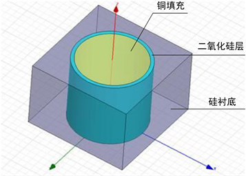
Figure 1. Model of cylindrical through silicon via
图1. 圆柱硅通孔模型
2. 圆柱硅通孔建模
目前,最常见的硅通孔结构呈圆柱体,如图1所示。
使用Q3D软件对不同尺寸的硅通孔进行仿真,得到半径为10 um时电阻参数值如图2所示。由图中数据可知,当频率低于107 Hz时,硅通孔的电阻值不发生变化,为直流电阻值,而随着频率的增加电阻值也随之增加,并且阻值增加的速率与硅通孔的尺寸有关。
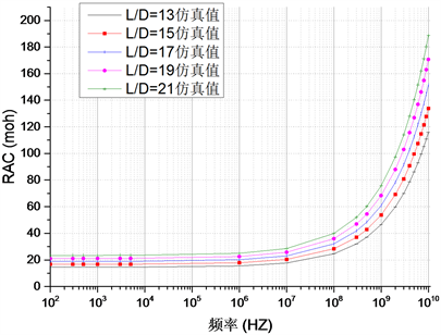
Figure 2. Simulation results of resistance and inductance of a cylindrical through silicon via with high aspect ratio
图2. 高面率比圆柱硅通孔电阻参数仿真结果电阻
3. 电阻参数提取解析式
3.1. 公式推导
圆柱形硅通孔电阻随频率变化可用公式(1)计算:
(1)
其中, 为硅通孔的直流电阻值,计算公式为:
(2)
为硅通孔中金属的电导率,L为硅通孔高度,r为硅通孔半径。
是频率为1 GHz时的电阻值,根据公式(1)可知,要想求出任意频率下的电阻值,需要先对频率为1 GHZ时的电阻值以及直流电阻进行求解,对于 的求解如下。
对于圆柱硅通孔,假定其内填充的金属导体是均匀、线性、各向同性的以及导体内部没有自由电荷,传导电流方向均沿Z轴,根据麦克斯韦–法拉第方程可得:
(3)
根据高斯定律,闭合曲面内总磁通量为零,结合旋度表示方法,电场的拉普拉斯算子可表达如下:
(4)
当传输信号为时谐场时,电场强度可表示为:
(5)
代入到式(4)中可以得到:
(6)
在圆柱硅通孔中,电场强度沿通孔方向,矢量方程可化为标量方程,进一步展开上述公式可得:
(7)
将式(7)展开之后得到齐次贝塞尔方程,根据电流密度的连续性,可知方程具有一阶贝塞尔函数性质:
(8)
其中, 为系数,和硅通孔尺寸参数有关,可以通过求解电流密度的积分得到; 是零阶第一类修正贝塞尔函数; 为趋肤深度,表达式分别为:
(9)
(10)
其中,I是在某一频率下,通过硅通孔的总电流,I1是一阶第一类修正贝塞尔函数,μ0为磁导率。
得出电场强度之后,就可以根据电流密度来计算硅通孔中电阻参数。
结合式(8)和(10)可得:
(11)
其中c为随趋肤深度度变化的常数,表达式为:
(12)
因为圆柱硅通孔金属导体内部只有沿Z轴的电流密度,通过对 进行积分便可得到电阻公式如下:
(13)
通过计算式(8)-(13)可得出:
(14)
为了进一步求解积分表达式的近似值,结合修正贝塞尔函数的近似表示可得:
(15)
式(15)为通过电、磁场强度以及麦克斯韦方程求解出的高频下电阻公式。
为了提高高频时电阻参数提取公式准确度,需要给定一个调整系数α。可以通过给定一个调整系数,从而使计算值和仿真值基本吻合,观察数据之间的关系,可给出频率为1 GHZ时电阻参数提取的调整系数 的表达式结构为:
(16)
式(16)中的未知数 以及 可通过曲线拟合的方法给出:
(17)
将式(17)与式(15)相乘,可以得到在频率为1 GHZ时,圆柱硅通孔的电阻表达式为:
(18)
将圆柱硅通孔模型尺寸参数代入到式(18)中,得到1 GHZ时的电阻计算值,与仿真值进行对比,发现误差极小,与仿真值对比发现两者基本吻合。
3.2. 解析式提取参数结果对比
将硅通孔模型尺寸参数分别代入到式(1)和(18)中,得到计算值,与仿真结果进行对比。高面率比下硅通孔电阻计算值和仿真值的对比结果如图3,图中数字代表的是面率比值。
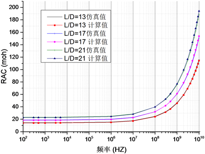
Figure 3. Comparison of resistance values with simulation values obtained by means of formula
图3. 解析式计算电阻值与仿真值对比
由图3中可以看出,根据公式(1)和(18)计算得出的电阻值与仿真结果之间有较好的契合度,且误差保持在5%以内,说明高面率比下圆柱硅通孔电阻参数提取公式有较高的准确度。
4. 结论
本文以高面率比圆柱硅通孔为研究对象,通过对不同尺寸参数下的圆柱硅通孔进行仿真,得到其寄生电阻参数值,使用拟合方法得到了高面率比圆柱形硅通孔的电阻参数解析式,解析式计算结果准确,误差在5%以内,满足精度要求。
文章引用
鞠艳杰. 三维集成电路中硅通孔电阻参数计算解析式提取的研究
Study on Extracting Analytical Formula for TSV Resistance Parameter Calculation in 3D IC[J]. 电路与系统, 2020, 09(03): 55-60. https://doi.org/10.12677/OJCS.2020.93008
参考文献
- 1. 邱碧秀. 微系统封装原理与技术[M]. 北京: 电子工业出版社, 2006.
- 2. Guarini, K.W. and TOPol, A.W. (2002) Electrical Integrity of State-of-the-Art 0.13 um SOI CMOS Devices and Circuits Transferred for Three-Dimensional (3D) Integrated Circuit (IC) Fabrication. The International Electron Devices Meeting, Hong Kong, 22 June 2002, 943-945.
- 3. Sakuma, K., Andry, P.S. and Tsang, C.K. (2008) 3D Chip-Stacking Technology with Through-Silicon Vias and Low-Volume Lead-Free Interconnections. IBM Journal of Research and Development, 52, 614-622. https://doi.org/10.1147/JRD.2008.5388567
- 4. Motoyoshi, M. (2009) Through-Silicon Via (TSV). Proceedings of the IEEE, 97, 43-48. https://doi.org/10.1109/JPROC.2008.2007462
- 5. Koyanagi, M. and Fukushima, T. (2009) High-Density through Silicon Vias for 3-D LSIs. Proceedings of the IEEE, 97, 49-59. https://doi.org/10.1109/JPROC.2008.2007463
- 6. Pavlidis, V.F. and Friedman, E.G. (2009) Interconnect-Based Design Methodologies for Three-Dimensional Integrated Circuits. Proceedings of the IEEE, 97, 123-139. https://doi.org/10.1109/JPROC.2008.2007473
- 7. Wong, B.P., Anurang, M. and Cao, Y. (2004) Nano-Cmos Circuit and Physical Design. John Wiley & Sons, New York. https://doi.org/10.1002/0471653829
- 8. Micael, J.T. and Jin, K. (1991) A Hybrid Method for the Calculation of the Resistance and Inductance of Transmission Lines with Arbitrary Cross Sections. Microwave Theory and Techniques, 39, 1338-1342. https://doi.org/10.1109/22.85409
- 9. Clayton, R.P. (1994) Analysis of Multiconductor Transmission Lines. John Wiley & Sons, New York.
- 10. Khalil, D.E., Ismail, Y., Khellah, M. and Karnik, T. (2008) Analytical Model for the Propagation Delay of Through Silicon Vias. 9th International Symposium on Quality Electronic Design, San Jose, CA, 17-19 March 2008, 553-556. https://doi.org/10.1109/ISQED.2008.4479795
- 11. Savidis, I. and Friedman, E.G. (2009) Closed-Form Expres-sions of 3-D Via Resistance, Inductance and Capacitance. IEEE Transactions on Electron Devices, 56, 1873-1881. https://doi.org/10.1109/TED.2009.2026200
- 12. Liang, Y.J. and Li, Y. (2011) Closed-Form Expressions for the Resistance and the Inductance of Different Profiles of Through-Silicon Vias. IEEE Electron Device Letters, 32, 393-395. https://doi.org/10.1109/LED.2010.2099203
- 13. Khaled, S., Ragai, H., Amin, K., et al. (2011) Compact Lumped Element Model for TSV in 3D-ICS. IEEE, 2321-2324.
- 14. Salah, K., El Rouby, A., Ragai, H., et al. (2012) A Closed Form Expression for TSV Based on Chip Spiralinductor. 2012 IEEE International Symposium on Circuits and Systems (ISCAS), Seoul, 20-23 May 2012, 2325-2328. https://doi.org/10.1109/ISCAS.2012.6271760