Optoelectronics
Vol.06 No.02(2016), Article ID:17827,5
pages
10.12677/OE.2016.62009
Resistance Characteristics Based on TiO2 Nanotube at Low Temperature
Yan Chen
Mathematical and Physical School, Mianyang Normal University, Mianyang Sichuan

Received: May 28th, 2016; accepted: Jun. 18th, 2016; published: Jun. 21st, 2016
Copyright © 2016 by author and Hans Publishers Inc.
This work is licensed under the Creative Commons Attribution International License (CC BY).
http://creativecommons.org/licenses/by/4.0/


ABSTRACT
This paper presents the TiO2 nanotube array (NTA) anodized. Use the carbon nanotube (CNT) film as the upper electrode coated on the TiO2 NTA, a CNT/TiO2NTA/Ti sandwich nanodevice has been fabricated. Its photoresponse and resistance characteristics at low temperature have been researched. Result shows that at 532 nm illumination, the photoconductivity of TiO2 NTA and the dark-conductivity have been strongly impacted by the temperature. The dark resistance and the photo resistance will decrease while the temperature rising, and the dark current and photoresponse accordingly increases as well. Finally, compared with other nanodevice used pre-electroforming, this result has been briefly studied.
Keywords:TiO2 NTA, Photoresponse, Dark Resistance

TiO2纳米管光电材料在低温下的阻变特性研究
陈燕
绵阳师范学院数理学院,四川 绵阳

收稿日期:2016年5月28日;录用日期:2016年6月18日;发布日期:2016年6月21日

摘 要
选用电化学阳极阳化方法在金属Ti片上生长了TiO2纳米管,并用碳纳米管(CNT)薄膜作为上电级,制作成了CNT/TiO2/Ti三明治形状的纳米器件。测试了样品在各低温下的光电响应特性和电阻特性。研究表明,选用碳纳米管作上电极的TiO2纳米管阵列,在532 nm的激光照射下,其光电导和暗电导特性极大地受到温度的影响。在低温下的光电阻和暗电阻会随着温度的增加而减小,同时暗电流增大,光响应度增强。最后,该器件和作了前置电阻处理后的同类型器件作了简要对比分析。
关键词 :TiO2纳米管,光响应,暗电阻

1. 引言
因其TiO2纳米管外形的独特性,自从2001年Gong D和其同事们首次报道了用HF溶液阳极阳化法生长出TiO2纳米管阵列以来,使TiO2纳米管在许多领域都得以应用,如超级电容器,太阳能电池,光催化降解和锂离子电池等,也因其对氢气和氧气的敏感,可用于制作如一些气体传感器。此外,用TiO2纳米管结合其它薄膜材料如碳纳米管,金属薄膜等组成异质结也可用于光电探测器的功能材料 [1] - [4] 。怎样降低暗电阻和提高光电响应度是光电探测器的研究的主要趋势,并在这基础之上扩宽对光的响应波长也是研究的重点内容。
为此,我们选用了Ti金属片,用阳极阳化的主法在其面上生长TiO2纳米管,并用碳纳米管薄膜用为上电级,以Ti片作为下电极,制作成了三明治形状的纳米器件。此前,我们对样品在常温下的光电响应特性作了研究,但其阻变前后在低温下的电阻及光响应特性测试并未进行。为此,我们分别测试了样品在阻变前的低温状态下的光电响应特性及电阻特性,并和未经阻变的其它上电极材料如石墨硒制作的同类型器件在低温下的性质作了简单的对比分析 [5] [6] 。
所有的低温测试均在高真空下进行,因样品对氧气和氢气的敏感,所以研究其在不同真空度下的对气体的光电响应特性也是现研究的热门,加之,经阻变处理后的样品薄膜在低温下电阻将作何改变是我们需要探讨的内容。
2. 实验过程
本样品采用阳极阳化两步生长法制备,并用石墨作为另一电极。第一步生长时加上60 V直流电压,用2400型真流源表监测,生长3小时后去掉氧化钛纳米管阵列(TiO2 NTA),再次生长。第二步选用30 V电压,生长25分钟,得到TiO2 NTA长度约为600纳米,内径约为20纳米,壁厚约为50纳米。如图1(a) SEM图像所示。
为了测试TiO2 NTA在光电流下的电阻,需简单制作一个光探测型的纳米器件。方法可在TiO2 NTA镀一层上电极,以Ti。金属作为下电极。曾经有报道,镀金或镀银电极都不如直接选用碳纳米管作为上电极要好,制方法简单又实惠 [7] 。为此,先将洗净的TiO2 NTA上表面四周用绝缘胶带覆盖,中间留出3 mm × 3 mm的透光窗口,再将由无序双壁碳纳米管(DWCNT)构成的厚度约为80 nm的薄膜铺在样品上表面,作为透明导电上电极。如图1(d)所示构成CNT/TiO2NTA/Ti三明治结构异质结构的纳米器件。
3. 分析及结果
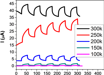
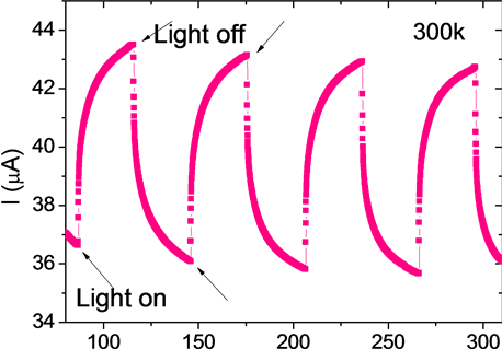
采用532纳米波长(光斑面积约为6.3 mm2;功率200 mW)的激光照射器件上表面的透光窗口,得到
有光照下的光响应曲线如图2(a)和图2(b)所示。图2(a)所示在常温300 K及20 V偏压下,光电流Ip达到0.044 mA,光照下电阻Rp约为0.45兆欧姆,暗电流为0.036 mA,暗电阻Rd约为0.55兆欧姆。图2(b)所示在20 V偏压下各低温下的光响应曲线。可以看出,随着温度的升高光电流及暗电流值均在增大。光响应电流(光电流和暗电流之差)也在增强。在100 K时的光响应最小。
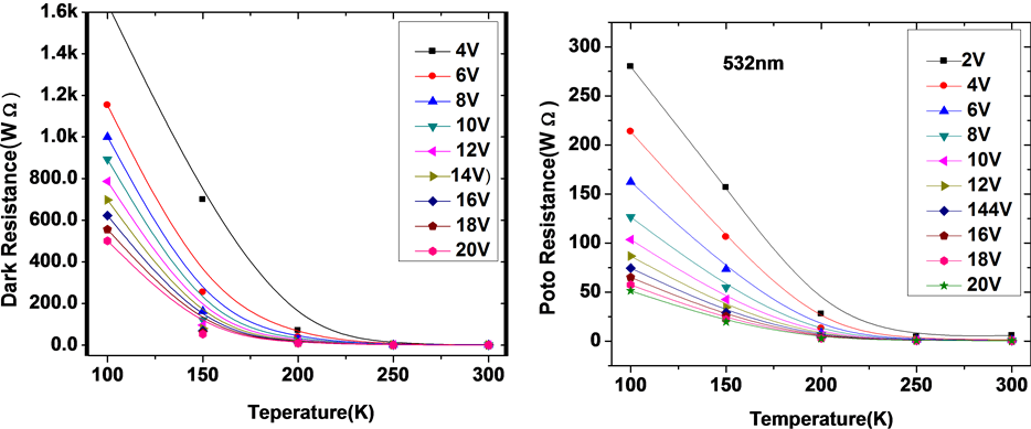
从图3(a)和图3(b)中可以看出,器件在各偏压下的光电阻和暗电阻均随温度的升高而减小。且所加电压越大,变化越不明显。经计算,在20 V偏压下100 K时,光电阻从300 K时的0.45兆欧增大为60.3兆欧,增大了近135倍。若偏压减小,电阻变化值越大。分析其原因可能是温度升高时增强了载流子的活性,加大了电流的输运速度,此结果和用石墨硒作上电极在低温下所测结果一致 [5] [6] 。因器件所能承受
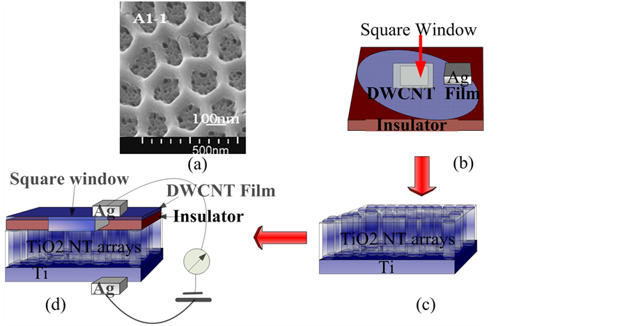
Figure 1. (a) The FESEM image of the TiO2 NTA surface; (b)-(d) Fabrication DWCNT/TiO2 NTA/Ti nano device process
图1. (a)为TiO2纳米管表面的扫描电镜图;(b)~(d)为DWCNT/TiO2 NTA/Ti器件的制作过程
 (a) t(s) (b) t(s)
Figure 2. (a) (b) The photoresponse of nanodevice at 532 nm illumination under the bias voltage of 20 V at different temperature
图2. (a) (b)分别为器件在532 nm,20 V各温度下的光响应
 (a)(b)
Figure 3. (a) The dark resistance of nanodevice at different temperature under the different bias voltage; (b) At 532 nm illumination the photo resistance of nanodevice at different temperature
图3. (a) 为器件在各偏压下的暗电阻随温度的变化关系图;(b) 为532 nm的光照下光电阻随温度的变化关系
的电压有限,若增至近40 V时,将发生阻变,即电流不再随电压的增大而变化,TiO2纳米管的电阻特性从高电阻形态改变至低电阻形态 [8] 。阻变后,光电流将大为增强,光电阻及暗电阻也相应地减小,其原因可能是在发生了阻变的纳米管内出现了一些空位丝,这样给载流子一个快速流通的通道 [9] - [11] ,这和升高温度有些近似。阻变后的电阻怎样随温度的变化而变化将是我们下一步研究的内容。这也为我们制作恒温下的光电器件提供一点启示和参考。
4. 结论
未经阻变处理的TiO2纳米管在低温下光电阻和暗电阻随着温度的降低而大大的增大,同时暗电流也会增大,光响应度增强,且和所加电压有关。电压越小变化将越显著。其结果为我们制作光电器件提供一些参考。
致谢
感谢清华大学物理系光电测试课题组在低温光响应测试方面所做的工作和指导。
文章引用
陈 燕. TiO2纳米管光电材料在低温下的阻变特性研究
Resistance Characteristics Based on TiO2Nanotube at Low Temperature[J]. 光电子, 2016, 06(02): 54-58. http://dx.doi.org/10.12677/OE.2016.62009
参考文献 (References)
- 1. Gong, D., Grimes, C.A., Varghese, O.K., Hu, W., Singh, R.S., Chen, Z. and Dickey, E.C. (2001) Titanium Oxide Nanotube Arrays Prepared by Anodic Oxidation. Journal of Materials Research, 16, 3331-3334. http://dx.doi.org/10.1557/JMR.2001.0457
- 2. Jun, Y., Jong, W., Parkwb, H. and Kang, M.G. (2012) The Preparation of Highly Ordered TiO2 Nanotube Arrays by an Anodization Method and Their Applications. Chemical Communications, 48, 6456-6471. http://dx.doi.org/10.1039/c2cc30733b
- 3. Tian, Y., Hu, C., He, X., Cao, C., Huang, G. and Zhang, K. (2010) Titania Nanotube Arrays for Light Sensor and UV Photometer. Sensors and Actuators B: Chemical, 144, 203. http://dx.doi.org/10.1016/j.snb.2009.10.065
- 4. Kang, Q., Lu, Q.Z., Liu, S.H., Yang, L.X., Wen, L.F., Luo, S.L. and Cai, Q.Y. (2010) A Ternary Hybrid CdS/Pt-TiO2 Nanotube Structure for Photoelectrocatalytic Bactericidal Effects on Escherichia coli. Biomaterials, 31, 3317-3326. http://dx.doi.org/10.1016/j.biomaterials.2010.01.047
- 5. Kang, Q., Yang, L., Chen, Y., Luo, S., Wen, L., Cai, Q. and Yao, S. (2010) Photoelectrochemical Detection of Pentachlorophenol with a Multiple Hybrid CdSexTe1−x/TiO2 Nanotube Structure-Based Label-Free Immunosensor. Analytical Chemistry, 82, 9749-9754. http://dx.doi.org/10.1021/ac101798t
- 6. Wang, M.-Z., Liang, F.-X., Nie, B. and Zeng, L.-H. (2013) TiO2 Nanotube Array/Monolayer Graphene Film Schottky Junction Ultraviolet Light Photodetectors. Particle & Particle Systems Characterization, 30, 630-636. http://dx.doi.org/10.1002/ppsc.201300040
- 7. Yang, M.J., Zhu, J.-L., Liu, W. and Sun, J.-L. (2011) Novel Photodetectors Based on Double-Walled Carbon Nanotube Film/TiO2 Nanotube Array Heterodimensional Contacts. Nano Research, 11, 0146. http://dx.doi.org/10.1007/s12274-011-0146-5
- 8. Zhang, G.W., Sun, J.-L., Wei, J.Q., Sun, H.H. and Zhu, J.-L. (2013) Significantly Enhanced Photoresponse in Carbon Nanotube Film/TiO2 Nanotube Array Heterojunctions by Pre-Electroforming. Nanotechnology, 24, Article ID: 465203.
- 9. Hu, W., Qin, N., Wu, G.H., Lin, Y.T., Li, S.W. and Bao, D.H. (2012) Opportunity of Spinel Ferrite Materials in Nonvolatile Memory Device Applications Based on Their Resistive Switching Performances. Journal of the American Chemical Society, 134, 14658-14661. http://dx.doi.org/10.1021/ja305681n
- 10. Hong, Q.S., Cao, Y., Xu, J., Lu, H.M., He, J.H. and Sun, J.-L. (2014) Self-Powered Ultrafast Broadband Photodetector Based on p-n Heterojunctions of CuO/Si Nanowire Array. ACS Applied Materials & Interfaces, 6, 20887-20894. http://dx.doi.org/10.1021/am5054338
- 11. Zhu, J.-L., Zhang, G.W., Wei, J.Q. and Sun, J.-L. (2012) Negative and Positive Photoconductivity Modulated by Light Wavelengths in Carbon Nanotube Film. Applied Physics Letters, 101, Article ID: 123117. http://dx.doi.org/10.1063/1.4754624