Advances in Condensed Matter Physics
Vol.04 No.02(2015), Article ID:15250,20
pages
10.12677/CMP.2015.42005
Research Progress in Positive Magnetoresistance System
Chan Gao, Jianwu Zhang*
Department of Physics, University of Science and Technology of China, Hefei Anhui
Email: *zjw@ustc.edu.cn
Received: May 3rd, 2015; accepted: May 18th, 2015; published: May 20th, 2015
Copyright © 2015 by authors and Hans Publishers Inc.
This work is licensed under the Creative Commons Attribution International License (CC BY).
http://creativecommons.org/licenses/by/4.0/


ABSTRACT
Over the last decade, the research of magnetoresistance effect and its mechanism has been one of the research hotspot of condensed matter physics. With the synthesis, preparation and discovery of a variety of new materials and new structural systems which possess magnetoresistance effect, its mechanism and the complexity of magnetoresistance system are also constantly being unfolded. In all kinds of magnetoresistance system and magnetoresistance effect which have been found, the research of positive magnetoresistance system and positive magnetoresistance effect, as a branch of the magnetoresistance research system, has special research value in the magnetoresistance system, magnetoresistance mechanism and application of new magnetoresistive devices. This paper reviews the progress of positive magnetoresistance system, magnetoresistance effect and its mechanism, shows the diversity of the positive magnetoresistance system, positive magnetoresistance effect and its mechanism, and briefly points out some common problems that need to be focused in the studies of the positive magnetoresistance system.
Keywords:Magnetoresistance, Positive Magnetoresistance, Linear Magnetoresistance, Extraordinary Magnetoresistance, Metal Particle Film, Diluted Magnetic Semiconductors, Topological Insulators, Semi-Metallic

正磁阻体系研究进展
郜婵,张建武*
中国科学技术大学物理系,安徽 合肥
Email: *zjw@ustc.edu.cn
收稿日期:2015年5月3日;录用日期:2015年5月18日;发布日期:2015年5月20日

摘 要
近十几年来,磁致电阻效应及其机理的研究一直是凝聚态物理领域的研究热点之一。随着具有磁阻效应的各种新材料及新结构体系的合成、制备与发现,磁阻体系及其磁阻机制的复杂性也不断被展现出来。在已发现的各类磁阻体系及磁阻效应中,正磁阻体系及正磁阻效应的研究,作为磁阻研究的一个分支,在磁阻体系、磁阻机理和新型磁阻器件应用方面,均具有特殊的研究价值。本文综述了正磁阻体系、正磁阻效应及其磁阻机理的研究进展,展示了正磁阻体系、正磁阻效应及其机理的多样性,并简要指出了正磁阻体系研究中需要关注的一些共性问题。
关键词 :磁致电阻,正磁阻效应,线性磁阻,超磁阻效应,金属颗粒膜,稀磁半导体,拓扑绝缘体,半金属

1. 引言
2007年10月,法国科学家阿尔贝费尔(Albert Fert)和德国科学家彼得·格林贝格尔(Peter Grunberg)因分别在铁/铬超晶格和铁/铬/铁三层膜结构中发现巨磁阻效应而共同获得2007年诺贝尔物理学奖,巨磁阻效应现已广泛应用于硬盘的磁头和各种传感器中,该效应引起了学术界的高度重视,巨磁阻效应成为凝聚态领域的研究热点之一。磁致电阻效应(Mgnetoresistance, MR)是指导体或半导体在磁场作用下电阻值发生变化的效应,表达式为:
 (1)
(1)
其中 和
和 分别表示外加磁场
 和不加磁场下的电阻率,磁阻值MR反映了体系电阻在加磁场和不加磁场下的变化。如果MR随磁场的增加而增加,则称该磁阻效应为正磁阻效应,反之,则称为负磁阻效应。磁阻效应按照其磁致电阻值的大小和产生机制的不同可以分为以下若干类别:
(1) 正常磁阻效应(Ordinary Magnetoresistance, OMR):OMR效应来源于磁场对电子的洛伦兹力,导致载流子在运动中发生偏转,使电子碰撞概率增加,引起附加的散射效应,从而使电阻值增大;OMR普遍存在于普通金属、合金及半导体材料中,这种磁电阻通常比较小。
(2) 各向异性磁阻效应(Anisotropic Magnetoresistance, AMR):AMR效应来源于电子的各向异性散射,铁磁性金属(Fe,Co,Ni及其合金)在磁场中发生磁化,从退磁状态到趋于饱和的过程中电阻发生变化的效应称为AMR;坡莫合金就是一种典型的各向异性磁阻材料,由于其在弱场下磁阻值较大,因此一般适用于弱场条件下。
(3) 巨磁阻效应(Giant Magnetoresistance, GMR):GMR效应是指磁性材料的电阻率在加场较之不加场时存在巨大的变化,通常可以达到10%,甚至100%以上;该效应源于自旋相关散射,多发生于多层膜、自旋阀、颗粒膜、非连续多层膜等材料体系中。
(4) 庞磁阻效应(Colossal Magnetoresistance, CMR):CMR主要发生于掺杂稀土金属氧化物材料体系中,这种材料体系的电阻率在外加磁场下会急剧变化,远远大于GMR,因此称为庞磁阻效应;CMR的发现极大地推进了磁传感器、高密度高速度磁存储器以及磁电子学的发展。
(5) 隧道磁阻效应(Tunneling Magnetoresistive, TMR):由于自旋相反的电子的隧穿几率不同而产生的磁阻效应称为隧道磁阻效应;TMR多发生在磁性层/非磁性层/磁性层的磁隧道结体系中,由于磁隧道结电阻率高,能耗小,性能比较稳定,因此有比较大的应用价值。
(6) 畴壁磁阻效应(Domain Wall Magnetoresistance, DWMR):畴壁磁阻效应源于位于畴壁中导电电子自旋散射与磁场的相关性;DWMR多发生于铁磁金属材料体系,由于铁磁金属畴壁结构比较复杂,磁电效应比较强,使得畴壁磁阻效应不容易被观察到,通过减去材料体系中比较明显的磁阻效应,可以观察到体系中微弱的畴壁磁阻,理论预计最大的畴壁磁阻可以达到250%。
(7) 弹道磁阻效应(Ballistic Magnetoresistance, BMR):当自旋极化的电子局限于自旋翻转的平均自由程可以与磁畴壁的宽度相比拟时,电子在加场后的电阻会迅速减小,这种效应称为弹道磁阻效应;BMR多发生于纳米接触中,源于发生于纳米接触的畴壁中的自旋相关散射。
(8) 隧道各向异性磁阻效应(Tunneling Anisotropic Magnetoresistance, TAMR),TAMR是在单一铁磁层的隧穿结构中发生的磁阻效应,源于自旋轨道耦合作用引起的态密度的各向异性;TAMR效应是一种较新的磁阻效应,还处于一个基础研究阶段,但其在自旋电子学领域有比较大的发展前景。
二十世纪六十年代,作为磁阻效应的一个分支,正磁阻效应逐渐受到越来越多研究者的关注。1969年,O. P. Katyal和A. N. Gerritsen在铬和铬–锌晶体中发现了正磁阻效应,他们将Zn作为掺杂物,研究了掺杂和温度对体系磁阻效应的影响[1] ;同年,G. E. Gurgenishvifi等人通过研究含有顺磁性杂质的金属,发现其在临界磁场下有正磁阻效应[2] ;1972,D. Kostopou通过对天然磁石的单晶进行研究,在温度达到临界点附近时,磁石单晶也会出现正磁阻效应[3] ;J. A. Rowlandst和S. B. Woods在对Pd-Rh合金的磁阻研究中发现随着Rh含量的变化,体系出现由正磁阻效应变为负磁阻效应的现象[4] 。由此可见,起初对正磁阻效应的研究多集中在合金、金属等材料体系,发生于合金、金属体系中的正磁阻效应,大多数可以归结为正常磁阻效应(OMR)。自二十世纪八十年代来,随着对正磁阻体系研究的深入,越来越多具有正磁阻效应的材料体系被挖掘出来,如在半导体[5] -[8] 、超导体[9] -[11] 、金属膜[12] [13] 、合金[14] [15] 、磁性半导体[8] [16] 、二维电子气体系[17] -[20] 、绝缘体[21] -[23] 以及金属间化合物[24] 等材料体系中均可以发现正磁阻效应的存在。
到目前为止,按照物理机制来划分,正磁阻效应的研究多集中于超磁阻效应(Extraordinary magnetoresistance, EMR)、线性磁阻效应(Linear Magnetoresistance, LMR)、隧道磁阻效应(TMR)、弹道磁阻效应(BMR)、畴壁磁阻效应(BWMR)、正常磁阻效应(OMR);按材料体系来分,对正磁阻效应的研究多集中于金属-半导体复合结构体系(如金属掺杂的半导体)、金属硫属化合物体系(如银硫属化合物)、拓扑绝缘体体系、半金属体系、铁磁金属体系、金属颗粒膜体系及异质结二维电子气等。
正磁阻效应作为磁阻效应研究的一个分支,正受到学术界越来越多的关注,具有正磁阻效应的材料体系也越来越多地得到开发和应用,如磁阻传感器[25] 、CPP巨磁阻头[26] 等。本文对不同机制的正磁阻效应以及不同材料体系的正磁阻效应从实验和理论两个方面进行了系统总结,并简要指出了正磁阻机制研究和正磁阻材料体系探索中需要关注的一些共性问题。
2. 几种正磁阻效应
2.1. 超磁阻效应(Extraordinary Magnetoresistance, EMR)
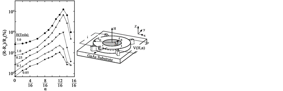
1998年,Solin等人发现,低场下,非均质半导体材料体系比均质半导体材料体系的巨磁阻效应更加显著,他们提出材料的巨磁阻效应与几何性质有着很大关联[27] -[30] 。2000年,Solin等人又发现在非磁性半导体InSb vdP盘中间嵌入一个电导率为 的导电不均匀的金(Au),这样的复合结构可以表现出异常
大的室温正磁阻效应[31] ,(如图1所示);在 时(其中
时(其中 为金属柱体的半径,
 为半导体的半径),磁场为0.05 T的条件下,其MR值可达到113%;而在
 时,在0.25 T和4 T的磁场下,MR
分别为9100%和750000%,这种异常大的正磁阻效应称为EMR (extraordinarily magnetoresistance)效应,由于这种效应与材料体系的几何因素有关,这种效应也可以称为几何磁阻效应。Solin等人指出这种异常大的正磁阻效应是因为当 ,磁导率张量为:
 (2)
(2)
 (3)
(3)
其中 为半导体中电子的迁移率
 (4)
(4)
 (5)
(5)
由(3)~(6)可知,在低场下,电流密度 平行于电场
平行于电场 ,因此电流将流过金属区域,此时金属区域相当于“短路”,而当高场时,
 不再平行于电场
 ,甚至垂直于电场,此时,电流会偏离金属区域,金属区域就相当于“开路”。如此,随着磁场由低场到高场,流经金属区域的电流将会发生由“短路”到“开路”的变化,这也是产生EMR的原因[32] 。
Solin等的这一发现引起了许多人对金属-半导体复合结构的研究,研究集中在其几何形状及电极位置以及材料选择对磁阻效应的影响。
2.1.1. 几何形状的改变对超磁阻效应的影响
Solin等发现的室温EMR,与诸多几何因素有关,比如:几何形状,电极位置等[6] 。T. H. Hewett和F. V. Kusmartsev用同样的材料,通过改变导电金属的几何形状,使正磁阻效应增加了近4个量级,他们用有限元的方法进行模拟计算得出电流在体系中的传输途径,发现这种正磁阻效应是加入磁场后电流的偏置所导致的[33] 。图2中(a)为Solin的实验图,(b)为T.H. Hewett和F. V. Kusmartsev通过改进后的实验图以及他们的结果,可以看出改进后,金属区域由圆盘改为“鱼骨”状,改进后的正磁阻值要远远大于vdP圆盘的正磁阻值,确切证实,改变金属的形状可以改变体系的磁阻效应。
Solin小组中的Lisa M. Pugsley等人将vdP圆盘结构,改用方形的金属嵌入[34] ,如图3所示,这样的改进可以在很大程度上增强正磁阻效应,在 时,磁阻可以达到107的数量级。他们在材料中间嵌入两个相距为d的金属结构(图4),同样可以达到很高的数量级。研究结果显示,适当改变金属区域的几何形状,可以在一定程度上增强正磁阻效应;可以预测,若把中间的金属区域分割的越多,正磁阻效应可能会越强。
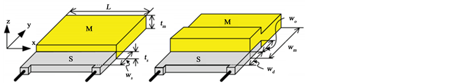
由于电极位置将直接影响电流在半导体和金属中的流通途径,因此,电极位置也是影响EMR的一个因素。当电极放置的位置不同,所产生的磁阻效应也不同[35] -[37] ,如[37] 中对比电极位置为VIVI和IVVI的分布,发现VIVI的分布方式可以显著增强磁阻效应,其灵敏度也显著提高;M. Oszwaldowski和S. El-Ahmar等人通过改变导电金属的位置以及电极的位置,构造出2D和3D的结构[38] ,如图5所示,
 (a) (b)
Figure 1. (a) The changing trend of magnetic resistance with radius ratio and magnetic field; (b) the experiment mechanism [31]
图1. (a) 磁阻随半径比α及磁场的变化趋势;(b) 实验机制[31]
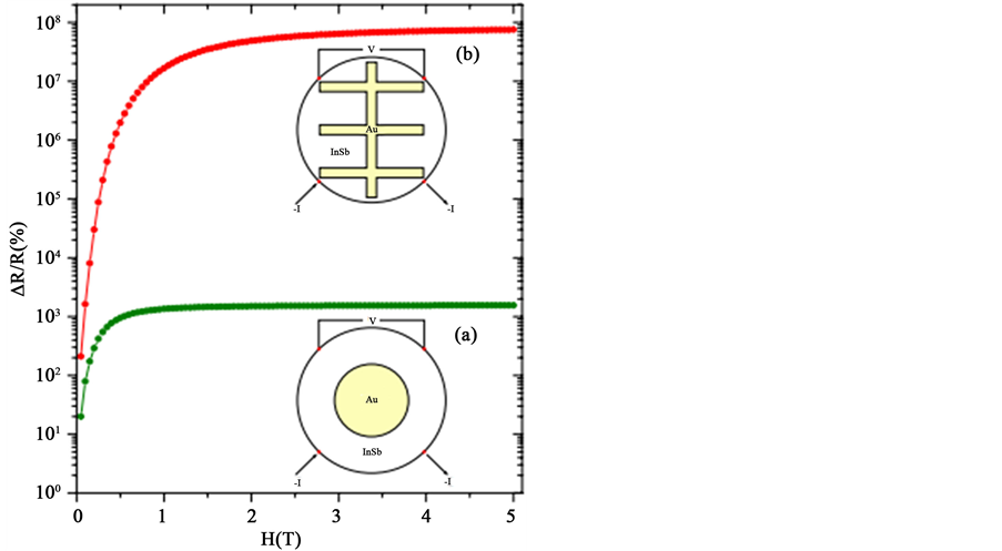
Figure 2. (a) vdP disc; (b) the improved experiment device of herringbone [33]
图2. (a) vdP圆盘;(b) 改进的鱼骨形的实验装置[33]
其中黄色部分M为导电非均匀金属区域,灰色S部分为半导体区域,1~4为四个电极端口。
他们的研究显示2D结构比3D结构的正磁阻效应更显著,原因是采用2D模式可以充分利用金属和半导体的异质结构,这种结构中金属绝缘体接触面积大,接触电阻比较小,相比而言,2D的结构更适合用于将来高质量的MR传感器。
半导体与金属之间的接触面积以及电极的接触电阻是影响体系正磁阻效应的另一个重要因素[37] 。Jian Sun和Jürgen Kosel最近研究了金属与半导体的接触面积对正磁阻效应的影响,他们的研究显示当金属部分的厚度 很小时,电流的z分量只存在于金属与半导体的接触面上,这样垂直磁场分量对磁阻没有贡献,磁阻较小;如图6所示,(黄色区域为金属材料,灰色为半导体),图6(b)中的重叠面积越大,越
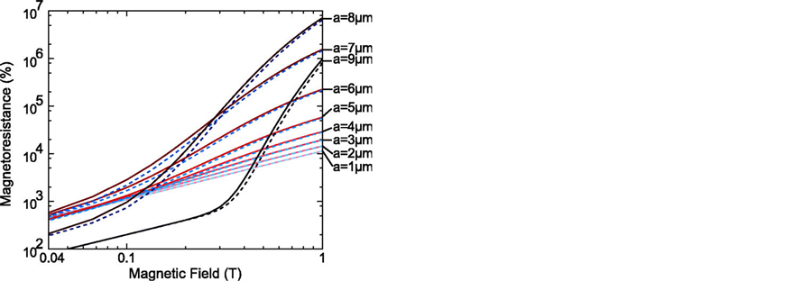
Figure 3. Replace the disk structure with square metal structure and its magnetoresistance effect [34]
图3. 以方形的金属代替圆盘结构以及其磁阻效应[34]

Figure 4. Divide the square metal area into two parts and its magnetoresistance effect [34]
图4. 将方形金属区域分为两部分及其磁阻效应[34]
 (a) (b)
Figure 5. (a) Standard 3D structure; (b) the improved 2D structure [34]
图5. (a) 标准的3D结构;(b) 改进的2D结构[34]
少的电流通过xz平面,半导体被短路,而z分量大多数存在于重叠的界面上,这样使得平行磁场分量对磁阻效应也有贡献;金属与半导体的接触面积越大,会使传感器的灵敏度降低,但是图6(b)中金属–半导体接触面积较大带来的灵敏度降低,会被金属–半导体之间良好的电流接触来弥补 [39] 。
通过改变金属–半导体复合结构中金属的形状、电极的位置、改变金属和半导体的接触面积都可以在很大程度上使磁阻发生变化。另外,将不同的结构(图7所示)对比发现EMR结构可以产生最大的低场MR,而Corbino结构则可以产生最大的高场MR。
 (a) (b)
Figure 6. The structure diagrams of metal and semiconductor (a) with different thickness; (b) with overlapping [39]
图6. (a) 金属与半导体厚度不同的结构图;(b) 金属与半导体有重叠[39]
 (a) (b)
Figure 7. (a) The Corbino geometric; (b) the EMR geometric [35]
图7. (a) Corbino 结构;(b) EMR结构[35]
2.1.2. 材料选用对超磁阻效应的影响
EMR的磁阻性质不仅与其几何结构及电极的位置有关,与其材料的选取也有很大关系。适用于EMR效应的材料大多数是高载流子的非磁性半导体,其中半导体的迁移率 对磁阻的影响较大。Matthias Holz等人用有限元方法(FEM)模拟并讨论了金属–半导体复合结构中材料的参数和接触电阻对正磁阻效应的影响,当金属的电阻率为
 时,金属的电导率与半导体的电导率相同,此时金属电阻率在
 附近发生一个微小的变化,就足以使总电阻和体系的灵敏度发生显著的变化;另外,载流子浓度的增加将导致半导体的电导率的增加,使总电阻降低,随着半导体的迁移率
 的增加,载流子的密度
 减少,因此,总体来说,具有高迁移率的半导体会显示出更明显的EMR效应,并且接触电阻越大,结构总体的性能越低[40] 。
另外,对于EMR材料的选择多使用窄带系的III-V族化合物,如InSb和InAs,因为这些化合物有较高的电子迁移率。文献[37] 用分子束外延生长的方法将 型的
型的 沉积在GaAs上,其中
 ,
, (300 K下),其磁阻可达到
 ,
, 。利用锑铟系列化合物的磁阻性质制成的元件已被投入到实际应用中,如半导体磁阻式电流传感器[41] 。
除了窄带系的III-V族化合物,二氧化硅和石墨烯等材料体系也表现出显著的正磁阻效应。Jianming Lu,Haijing Zhang等人在单层石墨烯上嵌入一个金属盘,构成EMR结构,如图8所示,发现在9T的磁场下,其正磁阻值可达到55000% [42] 。
在低场下,通过空穴掺杂和调节电流,轻度掺杂的二氧化硅会产生较显著的正磁阻效应,这种效应源于p-n边界产生的非均质性。在这个边界区域,体系的导电性由最多或最少的载流子决定(空穴与电子),加磁场后,这个边界区域内的电流发生变化,从而产生较大的磁阻效应,在0.07T的磁场下其磁阻可达
到10%,0.2 T下可达到100%,已经达到商业巨磁阻器件的性能要求[43] 。采用相似的结构,Michael P. Delmo等人发现,在0~3 T的磁场范围内,300 K下可以观察到一个近1000%的正磁阻,在20 K下,正磁阻可达到10000%;在电子载流子的浓度低于1013 cm−3时,在3~9 T磁场下的磁阻与磁场成正比关系,这种正磁阻效应主要发生在电场V > 50 V的区域,而一个相对较小、与磁场成二次相关的MR多发生在V = 25 V和50 V,如图9所示[44] [45] :
在对EMR的理论研究中,普遍采用的是Walf的理论和有限元模型,Walf提出半导体中高度导电的不均匀性确实可以增加Hall迁移率,从而导致载流子迁移率的改变[46] ,这种模型可以用来解释导电不均匀金属嵌入半导体结构的正磁阻效应[31] ;Solin等提出的有限元的模型,通过模拟电流在复合结构中的流通途径,可以解释之前金属-半导体复合结构的EMR实验结果[47] ,并且成功地将2D的结果延伸到3D [39] 。
2.2. 线性磁阻效应(Linear Magnetoresistance, LMR)
2.2.1. 银硫属化合物的线性磁阻效应
Ag2Se和Ag2Te是一种窄带隙自掺杂的n型半导体,高温 相,它们是快离子导体,电子输运是通过微观晶格畸变引起的耦合和离子迁移来实现的,但在低于一定温度(~400 K)时,离子的移动被冻结,成为非磁性半导体。结构转变为
 相的能带结构中,价带和导带之间存在一个百分之几电子伏的带隙,它们一般没有显著的磁阻效应,但是导带中的电子密度与化学计量比密切相关,小幅度改变一下它们的化学计量比,就会导致磁阻效应显著增加[48] 。如图10所示,在室温和近55KOe的磁场下,
 和
和

Figure 8. The EMR structure which is composed of a metal plate with single layer graphene embedded (the yellow area is metal, while the orange area is single layer graphene) and the corresponding magnetoresistance varies with the magnetic field [42]
图8. 单层石墨烯嵌入金属盘构成的EMR结构(黄色区域为金属,橙色区域为单层石墨烯)及体系相应的磁阻值随磁场的变化关系[42]
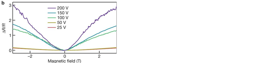
Figure 9. The positive magnetoresistance effect of intrinsic silicon (i-Si) when the temperature is 300 K [44]
图9. 本征硅(i-Si)的正磁阻效应(T = 300 K) [44]
 出现了奇特的磁阻效应,该磁阻可达200%,并且与磁场H成一个准线性的关系,在H = 60kOe下仍没有饱和的迹象,足以与庞磁阻材料相媲美,这种线性不饱和磁阻也称为线性磁阻(LMR) [48] 。正是由于这种磁阻效应的线性性质,使得其在磁性传感器方面的应用价值体现出来,而且使用非磁性材料可以在一定程度上弥补磁性材料在磁场中产生的巴克豪森效应。
Xu R.等的研究结果显示,银硫属化合物的磁阻效应不是由特殊的几何结构因素引起的[49] ,而是通过改变化合物的化学计量比所造成微观上的非均质而产生的。这种横向磁阻效应(MR⊥)在很宽的温度范围内保持线性[50] ,随着磁场线性增强,并在60T的磁场下未饱和,载流子的迁移率随着温度的降低而上升,这个规律同时适用于空穴掺杂和电子掺杂[49] 。Z. Ogorelec指出非化学计量比的银硫属化合物的正磁阻效应的最佳Hall迁移率为0.1 m2/Vs [51] ;B. Q. Liang提出在自掺杂的 薄膜中,当Ag的掺杂浓度
 时,会出现同时具有正磁阻和负磁阻效应的反常情况[52] 。
针对银硫属化合物的线性、不饱和的正磁阻效应,Abrikosov提出了量子LMR模型,指出LMR主要产生于在量子极限条件下有线性能量分布的无隙半导体中,而在银硫属化合物中随着温度的变化有一个由窄隙向无隙转变的一个过程,得出
 (6)
(6)
这个模型比较好地模拟出线性正磁阻效应,但未能很好的解释正磁阻效应与温度的关系[53] -[55] 。PL模型也可以用于解释银硫属化合物的线性磁阻效应,该模型中银硫属化合物的LMR可能是由于硫原子的非均质分布或迁移无序产生的,用随机电阻网格模型对其进行模拟并与实验结果进行比较,但PL模型
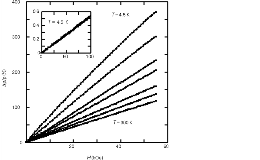
Figure 10. The relationship between normalized magnetoresistance of Ag2+δSe and magnetic field (from top to bottom, the temperature is 4.5, 30, 60, 90, 180, 270, 300 K; the illustration is the magnetoresistance when magnetic field is between 100 Oe) [48]
图10. Ag2+δSe归一化的磁阻与磁场的关系(由上至下T = 4.5,30,60,90,180,270,300 K;插图为在100 Oe磁场范围内的磁阻关系) [48]
仅限于在二维,不能对纵向磁阻进行模拟[56] [57] ,许洁等人对PL模型进行了延伸,并对纵向磁阻进行了模拟研究[49] 。S.A. Bulgadaev和F.V. Kusmartsev提出“random droplets”模型,也可以用来解释线性磁阻效应[58] 。Wang和Lei最近的研究指出LMR应该发生于有线性能量分布,并且在一个重叠的朗道能级下有一个非零 因子存在的2D体系中,他们的理论指出
 [59] 。对线性磁阻效应的诸多理论解释,都不能很好地解释全部的实验结果,对该效应的理论解释还需要进一步的研究。
2.2.2. 拓扑绝缘体的线性磁阻效应
拓扑绝缘体是一类具有新奇量子性质的材料,从能带结构上来看,它属于绝缘体,但拓扑绝缘体的表面存在一些特殊的量子态,其体电子态是有能隙的绝缘态,表面态则是无能隙的金属态。由于强自旋轨道耦合作用,表面态受到体能带结构的时间反演对称保护,不易受到体系中缺陷和杂质的影响。对拓扑绝缘体的研究已成为一个热点[60] -[62] ,其正磁阻效应的研究也引起特别关注[63] -[73] 。目前,该方面研究主要集中在拓扑绝缘体Bi2Se3和Bi2Te3上[67] -[72] ,研究显示,单个的Bi2Se3纳米片的载流子的霍尔迁移率高达 ,如图11所示,在14 T的磁场和1.4 K的温度下其正磁阻效应高达400%,在高温端300 K时其正磁阻效应也达75%,且没有饱和的趋势[67] 。
拓扑绝缘体的磁阻性质与其输运性质[66] [67] [71] 及载流子[67] 的浓度相关,也有研究指出拓扑绝缘体的磁阻效应与弱无序的存在而产生的2D EEI效应相关[70] ,可以用2D的WAL理论来解释。有研究指出在高指数(221)拓扑绝缘体Bi2Se3薄膜上发现了准二维的线性磁阻,不同于先前研究的与无隙线性能量分布直接相关的LMR效应,此处的LMR与无序直接相关[74] ;Wang等人在Bi2Se3纳米片上发现高达600%的室温正磁阻,并且在13 T的磁场下不饱和[65] 。拓扑绝缘体作为一种新材料,其在磁阻方面的性质将使其成为正磁阻体系研究的一个引人注目的分支。
2.3. 隧道磁阻效应(TMR)
隧道磁阻效应发生于隧道结中,所谓隧道结是将两层电导体由一个绝缘薄膜层连接起来形成三明治结构,在磁场作用下,隧道结会呈现出一种磁阻效应,该效应就是隧道磁阻效应。目前,这种效应多发生在磁隧道结(MTJ)中,磁隧道结是由被绝缘薄膜分隔的两铁磁层构成的,加磁场后,磁场会通过影响铁磁层中的磁化方向,从而对MTJ的电阻产生影响。
在对正磁阻效应的研究中,磁阻效应多是以公式(1)来定义的,而在隧道磁阻效应中磁阻的定义为:
 (7)
(7)
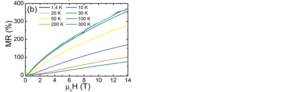
Figure 11. The MR curve of topological insulator Bi2Se3 nanosheet [67]
图11. 拓扑绝缘体Bi2Se3纳米片的MR曲线[67]
其中 和
和 分别表示两个电极的磁化方向反平行和平行排列时的隧道电阻,按定义(7)得到的是隧道磁阻效应,这种磁阻效应在室温下就可以达到很大的数值,因此也激发了对将隧道磁阻效应应用于磁传感器、读写头和其它电子元件领域中的研究。S. Yuasa团队在磁性隧道结(MTJs)中发现正的隧道磁阻效应,他们的研究显示在Fe/MgO/Fe的隧道结中有较大的正隧道磁阻效应[75] -[78] ,且这种磁阻效应与中间氧化层的厚度及温度等相关[75] ;S. Yuasa等还在Ga1-xMnxAs/ZnSe/Ga1-xMnxAs的异质结结构的磁性隧道结中发现了高达100%的正磁阻效应[77] ;Stuart S. P. Parkin等人发现以CoFe为电极的MgO (100)隧道结在低温下的隧道磁阻效应也可达300%,即使在室温下也可以呈现出高达220%的隧道磁阻效应[79] 。J. Mathon提出了针对隧道巨磁阻效应的紧束缚理论[80] ,但是这个理论可以用来解释Co (001)结一类的隧道磁阻效应,却不能用来定量或定性地解释所有的隧道磁阻效应,要找到一个适用于隧道磁阻效应的统一理论解释,还需要更多的研究。目前,对TMR效应的研究已从基础实验与理论方面进入到应用领域中[81] 。
2.4. 弹道磁阻效应(BMR)
隧道磁阻效应多是发生在隧道结中,当自旋极化的电子局限于自旋翻转的平均自由程可以与磁畴壁的宽度相比拟的区域时,电子在加磁场后的电阻会很快减小,这样产生的磁阻效应称为弹道磁阻效应(BMR)。BMR要比GMR和TMR大的多[82] 。弹道磁阻效应多发生在纳米点接触结构中,其中Ni纳米点接触结构已被详细研究。N. Garca等人在电沉积Ni-Ni纳米点接触结构中发现了低场下高达700%的室温弹道磁阻,并且远远大于GMR [83] ;Harsh Deep Chopra在Ni纳米点接触结构中观察到高达3000%的室温BMR [84] ,Susan Z. Hua在稳定的Ni纳米点接触结构中发现了100000%的室温弹道磁阻 [85] ,Matthew R. Sullivan等人则在没有磁致伸缩的Ni单原子导体中发现非常大的BMR [86] 。BMR磁阻值比较大,未来在高密度磁读写头及高灵敏磁传感器上可能会潜在的应用价值。
2.5. 正常磁阻效应(OMR)
非磁性金属材料中普遍存在着正常磁阻效应,通常,这种磁阻效应在低场下比较小,且无论在纵向磁场、还是在横向磁场中,正常磁阻效应的 。正常磁阻效应来源于载流子在运动中受到磁场引起的洛伦兹力,偏离了原来的运动轨迹,使电子碰撞概率增加,引起附加的散射效应,从而使电阻升高。这种磁阻效应多发生在普通金属、合金及半导体等体系中。
S. Honda等人对Co-Bi薄膜的研究发现,在该体系中OMR和AMR同时存在,其中OMR分支与Bi组分直接相关,OMR效应随着x (x为Co与Bi的厚度比)的增大而减小,在只有Bi膜组分时(即x=0),磁阻效应 ,此时的MR约为0.5%,可以用OMR效应来解释[87] 。OMR的发生多是源于霍尔效应,由于该磁阻效应与磁场直接相关,因此,可以通过增加有效磁场来增强体系中的OMR。在Co/Si体系中,将Si做阳极化处理后,在50 K的温度下通以垂直磁场,可以得到60%的OMR,该效应随着温度的上升而减弱,这可能是由于晶体Si的电阻随温度的变化而引起的[88] 。
正常磁阻效应源于载流子所受到的洛伦兹力,通常比较小,但是可以通过一些方法来增强正常磁阻效应,如可以通过增加有效磁场来增强OMR [88] 等。
2.6. 畴壁磁阻(DWMR)
从最早对铁金属须的研究开始,铁磁金属的畴壁的电性质及磁性质的研究受到越来越多的关注。由于铁磁金属畴壁的结构复杂,磁电效应会使一些表现微弱的性质不容易被观察到,如畴壁磁阻效应。为了克服这一难题,M. Viret等人通过减去AMR等较明显的磁阻效应,在Co和Ni中发现了这些微弱但非零的畴壁磁阻效应,并用基于 Larmor 进动理论的半经典模型对其进行解释[89] ;随后,Levy和Zhang对Viret的模型进行改进,使其成为大多数研究人员所采用的量子力学形式(LZ model) [90] 。A. Radulescu等人对Co和Ni纳米线的畴壁磁阻进行研究,结果显示,Ni的畴壁磁阻比Co的要小一个数量级[91] ;R. F. Sabirianov等人对铁磁Co纳米线的电、磁和输运性质进行了详细的计算,结果显示,畴壁磁阻随着畴壁宽度的增大而急速减小,最大的磁阻值预计可达到250% [92] 。近几年,R.G.S. Sofin等人在Fe3O4(110)异质外延膜上观察到正的反相界面畴壁磁阻,反相界面(APB)是薄膜在异质外延生长过程中所出现的结构缺陷,当磁场方向平行于[110] 的方向时,磁阻是正的,这可能是因为位于APB附近的斜交旋转的长度减小和自旋倾斜的增加所导致的[93] 。对畴壁磁阻效应的研究已有很多,但多数属于基础实验研究方面,真正偏于应用开发的例子很少,如何将畴壁磁阻材料的基础研究成果推向应用,是目前该领域有待解决的问题。
3. 其它材料体系的正磁阻效应
3.1. 金属颗粒膜
1982年,H. Hoffmann等人在Pt薄膜上发现各向异性的正磁阻效应[94] ;1984年,R. S. Markiewicz和C. J. Rollins在Pb超薄膜上发现各向异性、与温度相关的正磁阻效应,这种正磁阻效应的产生与电子较强的自旋轨道散射产生的局域效应有关[95] ;同年Alice E. White等人发现了镁薄膜的正磁阻现象,在0.1~10 K的温度范围内,低场下可以观察到由正磁阻效应向负磁阻效应的转变[96] 。H. Akinaga等人的研究显示MnSb颗粒膜同样具有巨大的正磁阻效应,当向薄膜提供的电压高于阈值电压时,电流大小会改变1000%,基于这种性质,MnSb颗粒膜可以用来作为磁阻开关的材料[97] 。对金属颗粒膜的研究显示,普通金属颗粒膜普遍具有正磁阻效应,仅考虑“载流子在磁场中受到洛伦兹力的作用”,来解释金属颗粒膜的正磁阻现象是不够的,还必须考虑所研究物质的特性,以及该物质在磁场下性质的变化,才能很好地解释金属颗粒膜的正磁阻效应。
3.2. 合金
合金中普遍存在正磁阻效应。1980年,Abhijit Mookerjee通过研究自旋玻璃合金AuFe发现,自旋玻璃合金体系AuFe、AuCr、AgCr、AgMn和CuMn都具有正磁阻效应。此外,他们还利用自旋玻璃的Edwards-Anderson模型,配以Boltzmann方程,得到了对自旋玻璃合金的磁阻效应的理论解释,但是不足之处在于,低场下的正磁阻效应无法用该模型解释[15] ;2009年,J. M. Barandiarán等人在Ni-Mn-Ga和Ni-Fe-Ga赫斯勒合金中,在马氏体转变附近,磁阻值可以达到峰值,这是转变点零场电阻率异常和加场后转变温度变换的综合影响[98] 。
3.3. 磁性及非磁性半导体
G. Schmidt等人的研究显示,将电子自旋极化电流由稀磁体注入非磁性半导体中,结果会产生一种新颖的正磁阻效应,实验中可以得到25%的正磁阻效应,当非磁性半导体的自旋反转长度足够长时,正磁阻效应理论值可达100% [99] ;在非磁性 -共轭半导体薄膜中也存在线性正磁阻效应,即使在室温和低场下这种磁阻效应也可以达到10% [100] 。不仅非磁性半导体具有正磁阻效应,在一些磁性半导体中也可以观察到正磁阻效应,如MnxGe1−x稀磁性半导体表现出与磁性杂质直接相关的正磁阻效应[101] ;FeSb2是一种窄带系半导体,其磁性性质接近于近磁性质或“Kondo”绝缘体FeSi,由于FeSb2的金属化也会出现正巨磁阻效应[102] 。磁性和非磁性材料的正磁阻性质的研究已得到应用,其中非磁性半导体,如II-IV族半导体,已被成功地应用于半导体组件中[103] 。M. Foygel通过研究原子的自旋相关散射,来解释磁性半导体在不同条件下产生正磁阻效应和负磁阻效应的原因[104] ;束缚磁极化子跃迁模型可以用来解释磁性半导体和纳米结构中的巨磁阻效应[105] ;M. El-Hilo用蒙特卡洛模型可以预测磁性颗粒的磁性与温度和时间的关系[106] 。
3.4. 半金属
半金属介于金属与非金属之间,在与非金属作用时常作为电子给予体,而在与金属作用时常作为电子接受体,它有两种不同的自旋取向的电子,其中一种自旋取向(取自旋向上)的电子的能带结构呈现金属性,另一种自旋取向(取自旋向下)电子的能带结构呈现绝缘体或半导体,半金属同时具有两种自旋取向电子,具备金属性和非金属性的性质。半金属的费米面附近的传导电子具有高达100%的自旋极化率,因此半金属材料是一种具有极大的应用潜能的自旋电子学材料 [107] 。
对于半金属的磁阻研究也有许多,Kai Liu等人研究了半金属Bi纳米线的正磁阻效应[108] ,D. X. Li等对半金属GdX (X = P, As, Sb, Bi)单晶的电子输运特性进行了研究,结果显示,在低温下横向磁阻 ,在10T的磁场下有非常大的正磁阻效应,表1中列出了不同半金属的晶格常数,尼尔温度,剩余磁阻等[109] 。
拓扑半金属YPtBi也具有非常规的正磁阻效应,这种磁阻效应对样品表面的粗糙度很敏感,这表明表面态是影响磁阻效应的一个重要因素,这种材料也成为拓扑超导体的候选材料之一[110] 。石墨纳米管束也是一种半金属,它在低温下的电导率 表现出二维的弱局域行为,此时会产生负磁阻效应,而当温度达到60 K时,其磁阻效应为正值,并且其电导率
 与温度成近线性关系[111] 。在高取向的热解石墨中,在T = 4.5 K,H = 8.15 T时,MR = 69400%,这是一个显著的正磁阻效应,而且在很宽的温度范围内发生半金属-绝缘体过渡转变,这种现象与磁场作用直接相关[112] 。高载流子迁移率的半导体和半金属通常会有正磁阻效应,S. Ishiwata等人发现多层半金属β-CuAgSe表现出显著的正磁阻效应和Shubnikov de Haas振荡,低温下的磁阻随迁移率的增加而增加,掺杂Ni后可以引起材料的化学无序和晶格无序,在一定程度上使得电子迁移率显著提高,高的电子迁移率和化学无序的兼容性与化学非均质相关[113] 。
半金属材料作为一种新型的自旋电子学材料,有很大的应用前景,但半金属材料的传导电子极化率受表面电子的影响较大,使得传导电子极化率很难被准确测量表征,因此半金属材料在磁阻效应方面还未能得到较好的开发与应用。
3.5. 铁磁材料
铁磁材料一直以来都是材料研究中的一个热点。2000年,N. Manyala等通过对铁磁体的研究发现了由量子干涉效应引发的正磁阻效应;低温下无序增强了电子-电子相互作用,当 时,
时, 合金的零场电阻率
 随温度连续增加,并且表现出随着外加磁场的增加,
 不仅在
不仅在 附近增加,在
Table 1. Lattice constant, Neel temperature, residual resistance ratio, carrier concentration, size dimension, preparation method of different semimetal [109]
表1. 不同半金属的晶格常数,尼尔温度,剩余电阻率,载流子浓度,尺寸大小,制备方法等[109]
 的所有区域都增加的实验现象[114] 。JavierGuevara [115] 和M. K. Chattopadhyay [116] 也观察到了
 体系中的正磁阻效应,其中M. K. Chattopadhyay在Fe0.55Co0.45Si中发现10%的正磁阻效应。A. T. Burkov等人则在
 合金中发现巨大的正磁阻效应,无序结构的
 合金是由增强泡利顺磁性YCo2和铁磁性GdCo2组成,该体系在
 附近出现非常大的正磁阻效应[117] 。铁磁性薄膜已在MEMS巨磁阻式高度压力传感器中得到应用[118] 。
3.6. 稀磁半导体
普通的半导体材料大部分都不具有磁性,如InP、GaN、GaAs、ZnO等,而具有磁性的材料如Fe、Co、Ni等及其化合物则多不具有半导体的性质,它们与半导体材料的表面势垒不能很好地相容。半导体可以通过少量p型或者n型掺杂,从而改变其特性,因此可以通过掺入磁性离子的方法来使半导体获得磁性。在GaAs、GaN、InP、ZnO等半导体中掺杂引入过渡金属(或稀土金属)等磁性离子,由于磁性离子与半导体导带中电子的自旋交换作用(sp-dexchange)以及过渡金属离子之间的自旋交换作用(d-dexchange),使得这些材料具有磁性。这种通过部分取代非磁性离子而产生的磁性与本征磁性有显著的区别,因此称其为“稀磁”。由磁性离子部分地代替非磁性阳离子所形成的一类新型半导体材料,称之为“稀磁半导体”,具有很多独特的性质和广泛的应用。
Y. Fukuma等人用溅射法将Co掺杂的ZnO薄膜沉积到玻璃衬底上,并在该体系中发现了近线性的低温正磁阻效应[119] ;Wenjie Liang等人在对Co掺杂的ZnO稀磁半导体纳米线的研究中也发现了正磁阻效应,这种正磁阻效应主要发生在低场下,s-d交换作用引起的导带自旋分裂可能是产生该正磁阻效应的主要原因[120] ;Qingyu Xu等人研究了由于s-d交换作用产生的正磁阻效应,结果显示正磁阻效应可达到124% [121] ;Y. F. Tian等人在用分子束外延方法制备的Co掺杂ZnO的外延膜中,同样观察到正磁阻效应,这种效应与电子波函数的收缩有很大的关系[122] ;在金属掺杂的TiO2材料体系中,经Co掺杂后TiO2材料可由半导体变为导体,并且在2K温度下呈现出近60%的正磁阻效应,这为TiO2功能材料的应用拓展了一个新领域[123] 。
3.7. 碳材料
金刚石的人工合成、石墨层间化合物的研究、富勒烯及碳纳米管的发现及研究都取得了令人瞩目的进展,关于碳材料的磁阻效应研究也愈来愈受关注。清华大学的章晓中团队研究了金属–碳复合材料的磁阻效应[124] - [127] : 复合材料在高场(3T < B < 8T)下出现与磁场成线性关系的正磁阻效应,这种磁阻效应在8T的磁场下不饱和[124] ;
 复合材料在室温下表现出44.1%的正磁阻效应,该磁阻与磁场的关系可以表示为
 ,其中n取决于Ni的浓度和温度[125] 。他们对于用PLD (pulsed laser deposition)方法制备正巨磁阻效应的铁、钴、镍与碳的复合材料已经申请了专利[128] -[130] 。另外,在无序的碳纳米带[131] 、掺杂的单层碳纳米管[132] 、碳纳米管[133] 以及超薄石墨薄片[134] 等中都观察到了非常大的正磁阻效应。碳材料的应用前景十分诱人,它们有着很优越的性能,如碳纳米管有着特殊的电学性质、优良的力学性能,掺杂的单层碳纳米管有着显著的正磁阻性质等;但要使碳材料的正磁阻效应获得广泛的应用还有很多问题亟待解决,未来还要进行更多的研究。
3.8. 异质结二维电子气
二维电子气是指电子气可以在二维方向自由移动,而在第三维上受到限制的现象,它是许多场效应器件(例如MOSFET、HEMT)工作的基础,二维电子气容易在异质结结构中获得。 掺杂的GaAs/AlxGa1-xAs异质结,具有变程跃迁的导电机制,在该异质结中包含有单层二维电子气;这个体系在平行磁场中具有正磁阻效应,磁场下二电子的自旋方向将反向,磁场下的自旋排列减少了上Hubbard带的占据数,这是产生正磁阻效应的原因[19] 。V. Renard等人在AlGaAs/GaAs异质结二维电子气中发现了显著的准经典正磁阻效应,该正磁阻效应
 的对应关系,其中α = 0.9~1.2 [20] ;D. G. Polyakov的理论模型可以定性地解释该实验结果,但该模型很难解释该类磁阻效应的所有细节[135] 。Scott Dietrich 和Sergey Vitkalov等人通过研究置于弱量化磁场中的含二维电子气的GaAs量子阱,同样观察到了正磁阻效应[18] ,这种效应可能是由电子在磁场中的量子(周期)性运动引起的[136] 。人们在含有高密度的二维电子气的Si-MOSFET结构中也发现了正磁阻效应[17] 。
3.9. 多层膜
Carlos Diaz-Pinto等人用离子注入法在石墨多层膜中掺入硼或碳原子,即引入短程无序,实验结果显示掺杂前的石墨多层膜中可以观察到正磁阻效应,而在掺杂后可以观察到负磁阻效应,离子注入前后磁阻的变化,突出了无序对磁阻的影响[137] 。J. J. H. M. Schoonus等人在硼掺杂的 Si-SiO2-Al结构中发现了高达10000%的正磁阻效应[138] 。在多层膜LaMn2Ge2和Fe3O4/SrTiO3/La0.7S0.3MnO3的异质结结构中,同样观察到了正磁阻效应[139] [140] 。B. L. Johnson提出了针对Fe/Cr多层膜的杂质产生的自旋相关散射,基于玻尔兹曼输运方程对该体系进行理论计算,若对铁层掺杂带来的散射反对称与Cr层相当,GMR不会急剧减小;若带来的散射反对称与Cr层相反,则GMR会急剧减小,由此可见,中间层掺杂带来的散射中心的数目和类型不同,直接影响磁阻效应的大小[141] 。
异质结结构多数情况下也是多层膜结构,异质结二维电子气的正磁阻效应在上一部分已做说明,还有其它的异质结结构的磁阻效应也很显著,如ZnO/La0.7Sr0.3MnO3异质结,H = 0.5T时MR = 53.9%,H = 0.3T时MR = 36.4% [142] 。在GaAs/AlxGa1-xAs的异质结结构中,观察到与GaAs层中受主杂质密度有关的正磁阻效应[143] 。在(La2/3Ba1/3MnO3/LaNiO3)10超晶格的外延氧化物异质结中也可以观察到正磁阻效应[144] 。对异质结的正磁阻研究并不仅限于基础理论研究,而且已被投入应用,如多层膜制成MOSFET结构已应用于自旋金属氧化物半导体场效应晶体管[145] 。
4. 总结和展望
正磁阻体系复杂多样,其代表性体系如金属–半导体复合结构体系、金属硫属化合物体系、拓扑绝缘体体系、半金属体系等,在一定条件下都展现出较显著的正磁阻效应。迄今,该研究领域已积累了大量实验数据和研究结果。然而,对正磁阻体系、正磁阻效应及其机理的理论研究还相对不足,直到目前为止还没有提出一个比较系统的理论来认识和解释大多数正磁阻体系及其磁阻效应。已经提出的多数理论只能定性或定量解释一种或一类正磁阻体系中的正磁阻性质。正磁阻体系、正磁阻效应及其机理的理论研究,需要而且有必要从结构与性质关系的角度,深入而系统地考察已发现的各类正磁阻体系的结构与微结构特征,归纳、分析和总结其结构、微结构与正磁阻性质之间的规律性关联,提出更具概括性和适用性的正磁阻理论,以指导探索新的正磁阻体系,推动该领域基础研究与应用研究两方面的发展。
基金项目
本工作感谢国家自然基金(Grant Nos. 11174265)的资助,以及中国科技大学固体微结构实验室老师和同学们的支持。
文章引用
郜 婵,张建武, (2015) 正磁阻体系研究进展
Research Progress in Positive Magnetoresistance System. 凝聚态物理学进展,02,34-54. doi: 10.12677/CMP.2015.42005
参考文献 (References)
- 1. Katyalt, O.P. and Gerritsen, A.N. (1969) Investigation of hall resistivity and magnetoresistance of cadmium and cad-mium-zinc crystals. Physical Review, 178, 1037-1042.
- 2. Gurgenishvifi, G.E., Kharadze, G.A. and Nersesian, A.A. (1969) On the theory of low-temperature magnetoresistance of metals with paramagnefic impurities. Journal of Low Temperature Physics, 1, 633-639.
- 3. Kostopoul, D. (1972) Magnetoresistance of magnetite. Physica Status Solidi (a), 9, 523-527.
- 4. Rowlands, J.A. and Woods, S.B. (1972) Low-field magnetoresistance of palladium alloys. Physical Review B, 6, 1162- 1168.
- 5. Khosla, B.P. and Fischer, J.R. (1970) Magnetoresistance in degenerate CdS: Localized magnetic moments. Physical Review B, 2, 4084-4097.
- 6. Schmidt, D.R., Petukhov, A.G., Foygel, M., Ibbetson, J.P. and Allen, S.J. (1999) Fluctuation controlled hopping of bound magnetic polarons in ErAs:GaAs nanocomposites. Physical Review Letters, 82, 823-826.
- 7. Lee, M., Rosenbaum, T.F., Saboungi, M.L. and Schnyders, H.S. (2002) Band-gap tuning and linear magnetoresistance in the silver chalcogenides. Physical Review Letters, 88, Article ID: 066602.
- 8. Hu, R.W., Thomas, K.J., Lee, Y., Vogt, T., Choi, E.S., Mitrović, V.F., Hermann, R.P., Grandjean, F., Canfield, P.C., Kim, J.W., Goldman, A.I. and Petrovic, C. (2008) Colossal positive magnetoresistance in a doped nearly magnetic semiconductor. Physical Review B, 77, Article ID: 085212.
- 9. Palstra, T.T.M., Menovsky, A.A. and Mydosh, J.A. (1986) Anisotropic electrical resistivity of the magnetic heavy- fermion superconductor URu2Si2. Physical Review B, 33, 6527-6530.
- 10. 张建武, 张权 (2009) 一种正巨磁电阻复合功能陶瓷材料及制备方法. 中国专利: CN 101481244A.
- 11. Coleridge, P.T. (1987) Magnetoresistance and growth of the coherent state in CeCu6. Journal of Physics F: Metal Physics, 17, L79-L85.
- 12. Markiewicz, R.S. and Rollins, C.J. (1984) Localization and electron-interaction effects in a two-dimensional metal with strong spin-orbit scattering: Pd films. Physical Review B, 29, 735-747.
- 13. Ji, W.J., Xu, J., Jiao, L., Wang, J.F., Gu, Z.B., Chen, Y.B., Zhou, J., Yao, S.H. and Zhang, S.T. (2013) The structures and positive magnetoresistance of metallic Sr2CrWO6 epitaxial thin film. Ceramics International, 39, 9305-9308.
- 14. Ruvalds, J. and Sheng, Q.G. (1988) Magnetoresistance in heavy-fermion alloys. Physical Review B, 37, 1959-1968.
- 15. Mookerjee, A. (1980) Magnetoresistance of spin-glass alloys. Journal of Physics F: Metal Physics, 10, 1559-1566.
- 16. Liu, X.C., Chen, Z.Z., Shi, E.W., Liao, D.Q. and Zhou, K.J. (2011) Room-temperature anomalous Hall effect and magnetroresistance in (Ga, Co)-codoped ZnO diluted magnetic semiconductor films. Chinese Physics B, 20, Article ID: 037501.
- 17. Shlimak, A.B., Golosov, D.I., Friedl, K.J. and Kravchenko, S.V. (2012) Influence of spin polarization on resistivity of a two-dimensional electron gas in Si MOSFET at metallic densities. EPL, 97, Article ID: 37002.
- 18. Dietrich, S., Vitkalov, S., Dmitriev, D.V. and Bykov, A.A. (2012) Quantum lifetime of two-dimensional electrons in a magnetic field. Physical Review B, 85, Article ID: 115312.
- 19. Shlimak, I., Khondaker, S.I., Pepper, M. and Ritchie, D.A. (2000) Influence of parallel magnetic fields on a single-layer two-dimensional electron system with a hopping mechanism of conductivity. Physical Review B, 61, 7253- 7256.
- 20. Renard, V., Kvon, Z.D., Gusev, G.M. and Portal, J.C. (2004) Large positive magnetoresistance in a high-mobility two-dimensional electron gas: Interplay of short- and long-range disorder. Physical Review B, 70, Article ID: 033303.
- 21. Wu, J., Peng, J.L., Hamilton, J.J. and Greene, R.L. (1994) Variable-range hopping and positive magnetoresistance in insulating Y1-xPrxBa2Cu3O7 crystals. Physical Review B, 49, 690-693.
- 22. Syzranov, S.V., Moor, A. and Efetov, K.B. (2012) Strong quantum interference in strongly disordered bosonic insulators. Physical Review Letters, 108, Article ID: 256601.
- 23. Nguyen, H.Q., Hollen, S.M., Stewart, M.D., Shainline, J., Yin, A.J., Xu, J.M. and Valles, J.M. (2009) Observation of giant positive magnetoresistance in a cooper pair insulator. Physical Review Letters, 103, Article ID: 157001.
- 24. Jammalamadaka, S.N., Mohapatra, N., Das, S.D. and Sampathkumaran, E.V. (2009) Enhancement of positive magnetoresistance following a magnetic-field-induced ferromagnetic transition in the intermetallic compound Tb5Si3. Physical Review B, 79, Article ID: 060403.
- 25. Leng, Q., Kaiser, C., Guo, Y.M., Pakala, M. and Mao, S.N. (2009) Magnetoresistive sensors having an improved free layer. US8498084 B1.
- 26. Saito, M., Nishiyama, Y., Ide, Y., Umetsu, E., Hasegawa, N. and Hayakawa, Y. (2010) CPP GMR head with antiferromagetic layer disposed at rear of ferromagnetic pinned layer. US7800867 B2.
- 27. Solin, S.A., Thio, T., Hines, D.R., Kawano, M., Oda, N. and Sano, M. (1999) Large enhancement of the giant magnetoresistance in inhomogeneous semiconductors: Dependence on magnetic field direction. Journal of Applied Physics, 85, 5789.
- 28. Thio, T., Solin, S.A., Bennett, J.W., Hines, D.R., Kawano, M., Oda, N. and Sano, M. (1998) Giant magnetoresistance in zero-band-gap Hg1-xCdxTe. Physical Review B, 57, Article ID: 12239.
- 29. Thio, T., Solin, S.A., Bennett, J.W., Hines, D.R., Kawano, M., Oda, N. and Sano, M. (1998) Giant magnetoresistance in Hg1-xCdxTe and applications for high density magnetic recording. Journal of Crystal Growth, 184, 1293-1296.
- 30. Thio, T. and Solin, S.A. (1998) Giant magnetoresistance enhancement in inhomogeneous semiconductors. Applied Physics Letters, 72, 3497-3499.
- 31. Solin, S.A., Thio, T., Hines, D.R. and Heremans, J.J. (2000) Enhanced room-temperature geometric magnetoresistance in inhomogeneous narrow-gap semiconductors. Science, 289, 1530-1532.
- 32. Solin, S.A., Thio, T. and Hines, D.R. (2000) Controlled GMR enhancement from conducting inhomogeneities in non-magnetic semiconductors. Physica B, 279, 37-40.
- 33. Hewett, T.H. and Kusmartsev, F.V. (2010) Geometrically enhanced extraordinary magnetoresistance in semiconductor-metal hybrids. Physical Review B, 82, Article ID: 212404.
- 34. Pugsley, L.M., Ram-Mohan, L.R. and Solin, S.A. (2013) Extraordinary magnetoresistance in two and three dimensions: Geometrical optimization. Journal of Applied Physics, 113, Article ID: 064505.
- 35. Rowe, A.C.H. and Solin, S.A. (2005) Importance of interface sampling for extraordinary resistance effects in metal semiconductor hybrids. Physical Review B, 71, Article ID: 235323.
- 36. Branford, W.R., Husmann, A., Solin, S.A., Clowes, S.K. and Zhang, T. (2005) Geometric manipulation of the high-field linear magnetoresistance in InSb epilayers on GaAs (001). Applied Physics Letters, 86, Article ID: 202116.
- 37. Holz, M., Kronenwerth, O. and Grundler, D. (2005) Enhanced sensitivity due to current redistribution in the Hall effect of semiconductor-metal hybrid structures. Applied Physics Letters, 86, Article ID: 072513.
- 38. Oszwaldowski, M., El-Ahmar, S. and Jankowski, J. (2012) Extraordinary magnetoresistace in planar configuration. Journal of Physics D: Applied Physics, 45, Article ID: 145002.
- 39. Sun, J. and Kosel, J. (2013) Influence of semiconductor/metal interface geometry in an EMR sensor. IEEE Sensors Journal, 13, 664-669.
- 40. Holz, M., Kronenwerth, O. and Grundler, D. (2003) Magnetoresistance of semiconductor-metal hybrid structures: The effects of material parameters and contact resistance. Physical Review B, 67, Article ID: 195312.
- 41. 黄钊洪 (1999) 锑-铟系化合物半导体磁阻式电流传感器及电流传感方法. 中国专利: CN 1235276A.
- 42. Lu, J.M., Zhang, H.J., Shi, W., Wang, Z., Zheng, Y., Zhang, T., Wang, N., Tang, Z.K. and Sheng, P. (2011) Graphene magnetoresistance device in van der Pauw geometry. Nano Letters, 11, 2973-2977.
- 43. Wan, C.H., Zhang, X.Z., Gao, X.L., Wang, J.M. and Tan, X.Y. (2011) Geometrical enhancement of low-field magnetoresistance in silicon. Nature, 477, 304-307.
- 44. Delmo, M.P., Yamamoto, S., Kasai, S., Ono, T. and Kobayashi, K. (2009) Large positive magnetoresistive effect in silicon induced by the space-charge effect. Nature, 457, 1112-1115.
- 45. Delmo, M.P., Kasai, S., Kobayashi, K. and Ono, T. (2009) Space-charge-effect-induced large magnetoresistance in silicon. Journal of Physics: Conference: Conference Series, 193, Article ID: 012001.
- 46. Wolfe, C.M., Stillman, G.E. and Ross, J.A. (1972) High apparent mobility in inhomogeneous semiconductors. Journal of the Electrochemical Society, 119, 250-255.
- 47. Moussa, J., Ram-Mohan, L.R., Sullivan, J., Zhou, T., Hines, D.R. and Solin, S.A. (2001) Finite-element modeling of extraordinary magnetoresistance in thin film semiconductors with metallic inclusions. Physical Review B, 64, Article ID: 184410.
- 48. Xu, R., Husmann, A., Rosenbaum, T.F., Saboungi, M.L., Enderby, J.E. and Littlewood, P.B. (1997) Large magnetoresistance in non-magnetic silver chalcogenides. Nature, 390, 57-60.
- 49. Jie, X.U. and Zhang, D.X. (2011) Longitudinal magnetoresistance and “Chiral” coupling in silver chalcogenides. Communications in Theoretical Physics, 55, 532-536.
- 50. Yang, F.X., Xiong, S.T., Xia, Z.C., Liu, F.X., Han, C. and Zhang, D.M. (2012) Two-step synthesis of silver selenide semiconductor with a linear magnetoresistance effect. Semiconductor Science and Technology, 27, Article ID: 125017.
- 51. Ogorelec, Z., Hamzic, A. and Basletic, M. (1999) On the optimization of the large magnetoresistance of Ag2Se. Europhysics Letters, 46, 56-61.
- 52. Liang, B.Q., Chen, X., Wang, Y.J. and Tang, Y.J. (2000) Abnormal magnetoresistance effect in self-doped Ag2+δTe thin films (δ ≤ 0.25). Physical Review B, 61, 3239-3242.
- 53. Abrikosov, A.A. (2003) Quantum linear magnetoresistance solution of an old Mystery. Journal of Physics A: Mathematical and General, 36, 9119-9131.
- 54. Abrikosov, A.A. (2000) Quantum linear magnetoresistance. Europhysics Letters, 49, 789-793.
- 55. Abrikosov, A.A. (1998) Quantum magnetoresistance. Physical Review B, 58, 2788-2794.
- 56. Parish, M.M. and Littlewood, P.B. (2003) Non-saturating magnetoresistance in heavily disordered semiconductors. Nature, 426, 162-165.
- 57. Parish, M.M. and Littlewood, P.B. (2005) Classical magnetotransport of inhomogeneous conductors. Physical Review B, 72, Article ID: 094417.
- 58. Bulgadaev, S.A. and Kusmartsev, F.V. (2005) Large linear magnetoresistivity in strongly inhomogeneous planar and layered systems. Physics Letters A, 342, 188-195.
- 59. Wang, C.M. and Lei, X.L. (2012) Linear magnetoresistance on the topological surface. Physical Review B, 86, Article ID: 035442.
- 60. 吕衍凤, 陈曦, 薛其坤 (2012) 拓扑绝缘体简介. 物理与工程, 1, 7-18.
- 61. 吕莉, 张敏, 杨立芹, 羊新胜, 赵勇 (2013) 拓扑绝缘体 Bi2Se3单晶体的研究进展. 材料导报A, 6, 7-12.
- 62. 李辉, 彭海琳, 刘忠范 (2012) 拓扑绝缘体二维纳米结构与器件. 物理化学学报, 10, 2423-2435.
- 63. Zhang, W., Yu, R., Feng, W.X., Yao, Y.G., Weng, H.M., Dai, X. and Fang, Z. (2011) Topological aspect and quantum magnetoresistance of β-Ag2Te. Physical Review Letters, 106, Article ID: 156808.
- 64. He, H.T., Liu, H.C., Li, B.K., Guo, X., Xu, Z.J., Xie, M.H. and Wang, J.N. (2013) Disorder-induced linear magnetoresistance in (221) topological insulatorBi2Se3 films. Applied Physics Letters, 103, Article ID: 031606.
- 65. Wang, X.L., Du, Y., Dou, S.X. and Zhang, C. (2012) Room temperature giant and linear magnetoresistance in topological insulator Bi2Te3 nanosheets. Physical Review Letters, 108, Article ID: 266806.
- 66. Tang, H., Liang, D., Qiu, R.L. and Gao, X.P. (2011) Two-dimensional transport-induced linear magneto-resistance in topological insulator Bi2Se3 nanoribbons. ACS Nano, 5, 7510-7516.
- 67. Yan, Y., Wang, L.X., Yu, D.P. and Liao, Z.M. (2013) Large magnetoresistance in high mobility topological insulator Bi2Se3. Applied Physics Letters, 103, Article ID: 033106.
- 68. Zhang, H.B., Yu, H.L., Bao, D.H., Li, S.W., Wang, C.X. and Yang, G.W. (2012) Weak localization bulk state in a topological insulator Bi2Te3 film. Physical Review B, 86, Article ID: 075102.
- 69. Hor, Y.S., Qu, D., Pong, N. and Cava, R.J. (2010) Low temperature magnetothermoelectric effect and magnetoresistance in Te vapor annealed Bi2Te3. Journal of Physics: Condensed Matter, 22, Article ID: 375801.
- 70. Chiu, S.P. and Lin, J.J. (2013) Weak antilocalization in topological insulator Bi2Te3 microflakes. Physical Review B, 87, Article ID: 035122.
- 71. Hamlin, J.J., Jeffries, J.R., Butch, N.P., Syers, P., Zocco, D.A., Weir, S.T., Vohra, Y.K., Paglione, J. and Maple, M.B. (2012) High pressure transport properties of the topological insulator Bi2Se3. Journal of Physics: Condensed Matter, 24, Article ID: 035602.
- 72. Kastl, C., Guan, T., He, X.Y., Wu, K.H., Li, Y.Q. and Holleitner, A.W. (2012) Local photocurrent generation in thin films of the topological insulator Bi2Se3. Applied Physics Letters, 101, Article ID: 251110.
- 73. Wang, C.M. and Lei, X.L. (2012) Linear magnetoresistance on the topological surface. Physical Review B, 86, Article ID: 035442.
- 74. He, H.T., Liu, H.C., Li, B.K., Guo, X. and Xu, Z.J. (2013) Disorder-induced linear magnetoresistance in (221) topological insulatorBi2Se3 films. Applied Physics Letters, 103, Article ID: 031606.
- 75. Yuasa, S., Nagahama, T., Fukushima, A., Suzuki, Y. and Ando, K. (2004) Giant room-temperature magnetoresistance in single-crystal Fe/MgO/Fe magnetic tunnel junctions. Nature Materials, 3, 868-871.
- 76. Nagahama, T., Yuasa, S., Tamura, E. and Suzuki, Y. (2005) Spin-dependent tunneling in magnetic tunnel junctions with a layered antiferromagnetic Cr(001) spacer: Role of band structure and interface scattering. Physical Review Letters, 95, Article ID: 086602.
- 77. Saito, H., Yuasa, S. and Ando, K. (2005) Origin of the tunnel anisotropic magnetoresistance in Ga1-xMnxAs/ZnSe/ Ga1-xMnxAs magnetic tunnel junctions of II-VI/III-V heterostructures. Physical Review Letters, 95, Article ID: 086604.
- 78. Saito, H., Yamamoto, A., Yuasa, S. and Ando, K. (2008) High tunneling magnetoresistance in Fe/GaOx/Ga1-xMnxAs with metal/insulator/semiconductor structure. Applied Physics Letters, 93, Article ID: 172515.
- 79. Parkin, S.S.P., Kaiser, C., Panchula, A., Ricei, P.M., Hughes, B., Samant, M. and Yang, S.H. (2004) Giant tunnelling magnetoresistance at room temperature with MgO (100) tunnel barriers. Nature Materials, 3, 862-867.
- 80. Mathon, J. (1997) Tight-binding theory of tunneling giant magnetoresistance. Physical Review B, 56, Article ID: 11810.
- 81. Yuan, L., Shen, J.X., Anderson, G.W. and Christopher, N.G. (2011) Method to improve reader stability and writer overwrite by patterned wafer annealing. US 20110102949 A1.
- 82. Chung, S.H., Munoz, M., Garcıa, N., Egelhoff, W.F. and Gomez, R.D. (2002) Universal scaling of ballistic magnetoresistance in magnetic nanocontacts. Physical Review Letters, 89, Article ID: 287203.
- 83. Garca, N., Muñoz, M., Qian, G.G., Rohrer, H., Saveliev, I.G. and Zhao, Y.W. (2001) Ballistic magnetoresistance in a magnetic nanometer sized contact: An effective gate for spintronics. Applied Physics Letters, 79, 4550-4552.
- 84. Chopra, H.D. and Hua, S.Z. (2002) Ballistic magnetoresistance over 3000% in Ni nanocontacts at room temperature. Physical Review B, 66, Article ID: 020403.
- 85. Hua, S.Z. and Chopra, H.D. (2003) 100,000 % ballistic magnetoresistance in stable Ni nanocontacts at room temperature. Physical Review B, 67, Article ID: 060401(R).
- 86. Sullivan, M.R., Boehm, D.A., Ateya, D.A., Hua, S.Z. and Chopra, H.D. (2005) Ballistic magnetoresistance in nickel single-atom conductors without magnetostriction. Physical Review B, 71, Article ID: 024412.
- 87. Honda, S. and Nagata, Y. (2003) Magnetic and transport properties of alternately deposited Co-Bi films. Journal of Applied Physics, 93, 5538.
- 88. Honda, S., Ishikawa, T., Takai, K., Mitarai, Y. and Harada, H. (2004) En-hanced ordinary magnetoresistance in Co/Si systems. Journal of Applied Physics, 96, 5915.
- 89. Viret, M., Vignoles, D., Cole, D. and Coey, J.M.D. (1996) Spin scattering in ferromagnetic thin films. Physical Review B, 53, 8464-8468.
- 90. Levy, P.M. and Zhang, S. (1997) Resistivity due to domain wall scattering. Physical Review Letters, 79, 5110-5113.
- 91. Radulescu, A., Ebels, U., Henry, Y., Ounadjela, K., Duvail, J.L. and Piraux, L. (2000) Magneto-resistance of a single domain wall in Co and Ni nanowires. IEEE Transactions on Magnetics, 36, 3062-3064.
- 92. Sabirianov, R.F., Solanki, A.K., Burton, J.D., Jaswaland, S.S. and Tsymbal, E.Y. (2005) Domain-wall magnetoresistance of Co nanowires. Physical Review B, 72, Article ID: 054443.
- 93. Sofin, R.G.S., Arora, S.K. and Shvets, I.V. (2011) Positive antiphase boundary domain wall magnetoresistance in Fe3O4 (110) heteroepitaxial films. Physical Review B, 83, Article ID: 134436.
- 94. Hoffmann, H., Hofmann, F. and Schoepe, W. (1982) Mag-netoresistance and non-ohmic conductivity of thin platinum films at low temperatures. Physical Review B, 25, 5563-5565.
- 95. Markiewicz, R.S. and Rollins, C.J. (1984) Localization and electron-interaction effects in a two-dimensional metal with strong spin-orbit scattering: Pd films. Physical Review B, 29, 735-747.
- 96. White, A.E., Dynes, R.C. and Garno, J.P. (1984) Low-temperature magnetoresistance in two-dimensional magnesium films. Physical Review B, 29, 3694-3696.
- 97. Akinaga, H., Mizuguchi, M., Ono, K. and Oshima, M. (2000) Room-temperature thousand fold magnetoresistance change in MnSb granular films: Magnetoresistive switch effect. Applied Physics Letters, 76, 357-359.
- 98. Barandiarán, J.M., Chernenko, V.A., Lázpita, P., Gutiérrez, J. and Feuchtwanger, J. (2009) Effect of martensitic transformation and magnetic field on transport properties of Ni-Mn-Ga and Ni-Fe-Ga Heusler alloys. Physical Review B, 80, Article ID: 104404.
- 99. Schmidt, G., Richter, G., Grabs, P., Gould, C., Ferrand, D. and Molenkamp, L.W. (2001) Large magnetoresistance effect due to spin injection into a nonmagnetic semiconductor. Physical Review Letters, 87, Article ID: 227203.
- 100. Mermer, Ö., Veeraraghavan, G., Francis, T.L., Sheng, Y., Nguyen, D.T., Wohlgenannt, M., Köhler, A., Al-Suti, M.K. and Khan, M.S. (2005) Large magnetoresistance in nonmagnetic π-conjugated semiconductor thin film devices. Physical Review B, 72, Article ID: 205202.
- 101. Li, A.P., Zeng, C., Benthem, K.V., Chisholm, M.F., Shen, J., Nageswara Rao, S.V.S., Dixit, S.K., Feldman, L.C., Petukhov, A.G., Foygel, M. and Weitering, H.H. (2007) Dopant segregation and giant magnetoresistance in manganese-doped germanium. Physical Review B, 75, Article ID: 201201.
- 102. Hu, R.W., Thomas, K.J., Lee, Y., Vogt, T., Choi, E.S., Mitrović, V.F., Hermann, R.P., Grandjean, F., Canfield, P.C., Kim, J.W., Goldman, A.I. and Petrovic, C. (2008) Colossal positive magnetoresistance in a doped nearly magnetic semiconductor. Physical Review B, 77, Article ID: 085212.
- 103. L莫伦坎普, G施米特 (2004) 具半磁性连接之半导体组件. 中国专利: CN 1509413A.
- 104. Foygel, M., Niggemann, J. and Petukhov, A.G. (2007) Atomic spin scattering and giant magnetoresistancein magnetic semiconductors. IEEE Transactions on Magnetics, 43, 3040-3042.
- 105. Petukhov, A.G. and Foygel, M. (2000) Bound magnetic polaron hopping and giant magnetoresistance in magnetic semiconductors and nanostructures. Physical Review B, 62, 520.
- 106. El-Hilo, M., Chantrell, R.W. and O’Grady, K. (1998) A model of interaction effects in granular magnetic solids. Journal of Applied Physics, 84, 5114-5122.
- 107. 任尚坤, 张凤鸣, 都有为 (2004) 半金属磁性材料. 物理学进展, 4, 381-397.
- 108. Liu, K., Chien, C.L. and Searson, P.C. (1998) Finite-size effects in bismuth nanowires. Physical Review B, 58, 14681- 14684.
- 109. Li, D.X., Haga, Y., Shida, H., Suzuki, T. and Kwon, Y.S. (1996) Electrical transport properties of semimetallic GdX single crystals (X=P, As, Sb, and Bi). Physical Review B, 54, 10483-10491.
- 110. Butch, N.P., Syers, P., Kirshenbaum, K., Hope, A.P. and Paglione, J. (2011) Superconductivity in the topological semimetal YPtBi. Physical Review B, 84, Article ID: 220504.
- 111. Song, S.N., Wang, X.K., Chang, R.P.H. and Ketterson, J.B. (1994) Electronic properties of graphite nanotubules from galvanomagnetic effects. Physical Review Letters, 72, 697-700.
- 112. Wang, Z.M., Xing, D.Y., Zhang, S.Y., Xu, Q.Y., Van Beal, M. and Du, Y.W. (2007) Magnetic-field-induced semimetal-insulator-like transition in highly oriented pyrolitic graphite. Chinese Physics Letters, 24, 199-202.
- 113. Ishiwata, S., Shiomi, Y., Lee, J.S., Bahramy, M.S., Suzuki, T., Uchida, M., Arita, R., Taguchi, Y. and Tokura, Y. (2013) Extremely high electron mobility in a phonon-glass semimetal. Nature Materials, 12, 512-517.
- 114. Manyala, N., Sidis, Y., Di Tusa, J.F., Aeppli, G., Young, D.P. and Fisk, Z. (2000) Magnetoresistance from quantum interference effects in ferromagnets. Nature, 404, 581-584.
- 115. Guevara, J., Vildosola, V., Milano, J. and Llois, A. (2004) Half-metallic character and electronic properties of inverse magnetoresistant Fe1-xCoxSi alloys. Physical Review B, 69, Article ID: 184422.
- 116. Chattopadhyay, M.K., Roy, S.B., Chaudhary, S., Singh, K.J. and Nigam, A.K. (2002) Magnetic response of Fe1-xCoxSi alloys: A detailed study of magnetization and magnetoresistance. Physical Review B, 66, Article ID: 174421.
- 117. Burkov, A.T., Zyuzin, A.Y., Nakama, T. and Yagasaki, K. (2004) Anomalous magnetotransport in (Y1-xGdx)Co2 alloys: Interplay of disorder and itinerant metamagnetism. Physical Review B, 69, Article ID: 144409.
- 118. 李孟委, 刘泽文, 刘双红, 孙剑文 (2012) MEMS巨磁阻式高度压力传感器. 中国专利: CN 202853815 U.
- 119. Fukuma, Y., Odawara, F., Asada, H. and Koyanagi, T. (2008) Effects of annealing and chemical doping on magnetic properties in Co-doped ZnO films. Physical Review B, 78, Article ID: 104417.
- 120. Liang, W.J., Yuhas, B.D. and Yang, P.D. (2009) Magnetotransport in Co-Doped ZnO nanowires. Nano Letters, 9, 892- 896.
- 121. Xu, Q.Y., Hartmann, L. and Schmidt, H. (2007) S-d exchange interaction induced magnetoresistance in magnetic ZnO. Physical Review B, 76, Article ID: 134417.
- 122. Tian, Y.F., Yan, S.S., Cao, Q., Deng, J.X., Chen, Y.X., Liu, G.L., Mei, L.M. and Qiang, Y. (2009) Origin of large positive magnetoresistance in the hard-gap regime of epitaxial Co-doped ZnO ferromagnetic semiconductors. Physical Review B, 79, Article ID: 115209.
- 123. Matsumoto, Y., Murakami, M., Shono, T., Hasegawa, T., Fukumura, T., Kawasaki, M., Ahmet, P., Chikyow, T., Koshihara, S. and Koinuma, H. (2001) Room-temperature ferromagnetism in transparent transition metal-doped titanium dioxide. Science, 291, 854-856.
- 124. Xue, Q.Z., Zhang, X. and Zhu, D.D. (2003) Room-temperature positive magnetoresistance in micro-sized Cox-C1-x composites. Physica B, 334, 216-220.
- 125. Xue, Q.Z. and Zhang, X. (2003) Positive magnetoresistance in micro-sized granular Nix-C1–x composites. Physics Letters A, 313, 461-466.
- 126. Xue, Q.Z., Zhang, X. and Zhu, D.D. (2004) Positive linear magnetoresistance in Fex-C1-x composites. Journal of Magnetism and Magnetic Materials, 270, 397-402.
- 127. Zhang, X., Xue, Q.Z. and Zhu, D.D. (2004) Positive and negative linear magnetoresistance of graphite. Physics Letters A, 320, 471-477.
- 128. 章晓中, 薛庆忠, 田鹏 (2004) 用PLD法制备具有室温正巨磁阻效应的镍碳薄膜材料. 中国专利: CN1487115A.
- 129. 章晓中, 薛庆忠, 朱丹丹 (2003) 用PLD方法制备具有正巨磁阻效应的铁碳薄膜材料. 中国专利: CN 1421941A.
- 130. 章晓中, 朱丹丹, 薛庆忠 (2003) 用PLD方法制备具有正巨磁阻效应的钴碳薄膜材料. 中国专利: CN 1412572.
- 131. Poumirol, J.M., Cresti, A., Roche, S., Escoffier, W., Goiran, M., Wang, X., Li, X.L., Dai, H.J. and Raquet, B. (2010) Edge magnetotransport fingerprints in disordered graphene nanoribbons. Physical Review B, 82, Article ID: 041413.
- 132. Vavro, J., Kikkawa, J.M. and Fischer, J.E. (2005) Metal-insulator transition in doped single-wall carbon nanotubes. Physical Review B, 71, Article ID: 155410.
- 133. Suzuura, H. and Ando, T. (2002) Phonons and electron-phonon scattering in carbon nanotubes. Physical Review B, 65, Article ID: 235412.
- 134. Weevelt, R.V., Mortet, V., Haen, J., Ruttens, B., Haesendonck, C.V., Partoens, B., Peeters, F.M. and Wagner, P. (2011) Study on the giant positive magnetoresistance and Hall effect in ultrathin graphite flakes. Physica Status Solidi A— Applications and Materials Science, 208, 1252-1258.
- 135. Polyakov, D.G., Evers, F., Mirlin, A.D. and Wolfle, P. (2001) Quasiclassical magnetotransport in a random array of antidots. Physical Review B, 64, Article ID: 205306.
- 136. Vavilov, M.G., Dmitriev, I.A., Aleiner, I.L., Mirlin, A.D. and Polyakov, D.G. (2004) Compressibility of a two-dimensional electron gas under microwave radiation. Physical Review B, 70, Article ID: 161306.
- 137. Diaz-Pinto, C., Wang, X.M., Lee, S., Hadjiev, V.G., De, D., Chu, W.K. and Peng, H.B. (2011) Tunable magnetoresistance behavior in suspended graphitic multilayers through ion implantation. Physical Review B, 83, Article ID: 235410.
- 138. Schoonus, J.J.H.M., Bloom, F.L., Wagemans, W., Swagten, H.J.M. and Koopmans, B. (2008) Extremely large magnetoresistance in boron-doped silicon. Physical Review Letters, 100, Article ID: 127202.
- 139. Mallik, R., Sampathkumaran, E.V. and Paulose, P.L. (1997) Large positive magnetoresistance at low temperatures in a ferromagnetic natural multilayer, LaMn2Ge2. Applied Physics Letters, 71, 2385-2387.
- 140. Ghosh, K., Ogale, S.B., Pai, S.P., Robson, M., Li, E., Jin, I., Dong, Z.W., Greene, R.L., Ramesh, R., Venkatesan, T. and Johnson, M. (1999) Positive giant magnetoresistance in a Fe3O4/SrTiO3/La 0.7Sr0.3MnO3 heterostructure. Applied Physics Letters, 73, 689-691.
- 141. Johnson, B.L. and Camley, R.E. (1991) Theory of giant magnetoresistance effects in Fe/Cr multilayers: Spin-dependent scattering from impurities. Physical Review B, 44, 9997-10002.
- 142. Jin, K.X., Zhao, S.G., Chen, C.L., Wang, J.Y. and Luo, B.C. (2008) Positive colossal magnetoresistance effect in ZnO/La0.7Sr0.3MnO3 heterostructure. Applied Physics Letters, 92, Article ID: 112512.
- 143. Heisz, J.M. and Zaremba, E. (1996) Transverse magnetoresistance of GaAs/AlxGa1-xAs heterojunctions in the presence of parallel magnetic fields. Physical Review B, 53, 13594-13604.
- 144. Nikolaev, K.R., Dobin, A.Y., Krivorotov, I.N., Cooley, W.K., Bhattacharya, A., Kobrinskii, A.L., Glazman, L.I., Wentzovitch, R.M., Dan Dahlberg, E. and Goldman, A.M. (2000) Oscillatory exchange coupling and positive magnetoresistance in epitaxial oxide heterostructures. Physical Review Letters, 85, 3728-3723.
- 145. 齐藤好昭, 杉山英行, 井口智明 (2008) 自旋金属氧化物半导体场效应晶体管. 中国专利: CN 101140952A.